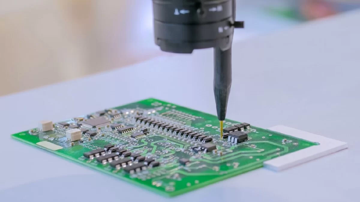
This article will provide a detailed overview of the types, causes, methods, and procedures of PCB solder pad repair, aiming to serve as a comprehensive reference for electronic engineers and technicians.Printed Circuit Boards (PCBs) are crucial components in modern electronic devices.
Types and Causes of Solder Pad Damage
Mechanical Damage: Includes scratches, dents, and fractures, usually caused by improper handling or accidental impact.
Thermal Damage: Occurs when the soldering temperature is too high or the heating time is too long, leading to solder pad detachment from the PCB or deformation.
Chemical Corrosion: Happens when solder pads come into contact with corrosive chemicals, resulting in surface corrosion spots or solder pad detachment.
Soldering Defects: Includes poor soldering, voids, and incomplete solder joints.
These damages directly affect the connection of electronic components and the performance of the circuit board, necessitating appropriate repair methods.
PCB Solder Pad Repair Methods
1.Depending on the type and extent of damage, the repair methods can be divided into the following categories:
Solder Pad Reflow Method: Suitable for minor soldering defects and surface scratches.
Clean the Solder Pad: Use alcohol and a cleaning brush to clean the surface of the solder pad, removing oxides and residues.
Apply Flux: Evenly apply flux on the solder pad to help the solder adhere better.
Reflow Solder: Use a soldering iron to heat the solder wire and reflow solder on the pad, ensuring the solder evenly covers the pad surface.
Cool and Clean: After reflow, allow the solder to cool and clean the pad surface again with alcohol.

PCB Solder Pad Repair
2.Solder Pad Replacement Method: Suitable for severe mechanical and thermal damage.
Remove the Damaged Pad: Use a hot air gun to heat the damaged pad until the solder melts, then remove the pad with tweezers.
Clean the PCB Surface: After removing the pad, clean the PCB surface with cleaning tools to ensure no residual solder or dirt.
Place the New Pad: Place a new pad on the PCB, ensuring accurate positioning.
Solder the New Pad: Use a soldering iron and solder wire to solder the new pad in place, ensuring a firm connection.
Inspect and Test: After soldering, perform visual inspection and electrical testing to ensure the pad connection is good.
3.Conductive Adhesive Repair Method: Suitable for chemical corrosion and mild damage.
Clean the Pad Surface: Clean the surface of the pad with cleaning tools to ensure no dirt or oxides.
Apply Conductive Adhesive: Apply an appropriate amount of conductive adhesive to the damaged area, ensuring even coverage.
4.Cure the Conductive Adhesive: Place the PCB in an oven according to the adhesive's instructions for curing.
Inspect and Test: After curing, perform visual inspection and electrical testing to ensure the repaired pad has good conductivity.
5.Rebuild Pad Method: Suitable for completely detached pads or large area damage.
Clean and Prepare: Clean the damaged area to ensure no residual solder or dirt.
Place Conductive Copper Foil: Cut an appropriate piece of conductive copper foil according to the damaged area and place it in the damaged position.
Fix the Copper Foil: Use conductive adhesive to fix the copper foil in place, ensuring accurate positioning.
Solder the Copper Foil: Use a soldering iron and solder wire to solder the edges of the copper foil, ensuring a firm connection with the PCB.
Cure and Clean: Wait for the conductive adhesive to cure, then clean the pad surface to ensure smoothness.
Inspect and Test: Perform visual inspection and electrical testing to ensure the rebuilt pad functions properly.
Precautions in PCB Solder Pad Repair
Temperature Control: Strictly control the soldering temperature during repair to avoid overheating and damaging the PCB.
Cleaning Work: Thoroughly clean before and after each step to prevent residual substances from affecting the repair.
Tool Selection: Choose appropriate tools and materials to ensure smooth repair process.
Electrical Testing: Perform electrical testing after repair to ensure the pad connection is normal and there are no short circuits or open circuits.
Case Studies of PCB Solder Pad Repair
Case Study 1: Repair of Mechanical Damage
During production, an operator accidentally scratched a PCB solder pad, preventing the component from soldering properly. The technician decided to use the solder pad reflow method for repair.
Steps:
Clean the pad to remove surface dirt.
Apply flux to ensure even distribution of solder.
Use a soldering iron and solder wire to reflow solder, filling the scratch.
After cooling, perform visual inspection to ensure the pad surface is smooth and free of defects.
Result: After repair, the component was successfully soldered, and the circuit board functioned normally.
Case Study 2: Repair of Thermal Damage
During an overheating operation, a PCB solder pad detached. The technician decided to replace the pad.
Steps:
Use a hot air gun to heat and remove the detached pad.
Clean the PCB surface to remove residual solder.
Place a new pad and use a soldering iron and solder wire to fix it.
Perform visual inspection and electrical testing to ensure the pad connection is normal.
Result: The new pad was successfully replaced, and the circuit board functioned normally.
PCB solder pad repair is a highly technical task requiring rich experience and skillful techniques. Whether it is minor soldering defects or severe mechanical and thermal damage, appropriate methods can be used for repair. By following the various repair methods and specific procedures introduced in this article, technicians can effectively handle various solder pad damage issues in actual work, ensuring the normal operation of electronic devices.