
Enclosure for pcb board plays a crucial role in the design and manufacturing of PCBs.In the electronics manufacturing industry, PCB (Printed Circuit Board) is the core component of any electronic device. The task of PCB packaging involves how electronic components are encapsulated and installed on these boards. PCB packaging is about encapsulating electronic components into standard shapes and pin configurations, making them easy to insert or solder onto the PCB board. This article will guide you through the types of PCB packaging, application scenarios, and practical operations.
Proper PCB packaging can protect electronic components, enhance performance, reduce circuit noise and cross-interference, and ensure the stability and reliability of the entire circuit.Additionally,reasonable PCB packaging can save space and cost on the PCB board and increase the freedom of circuit design.

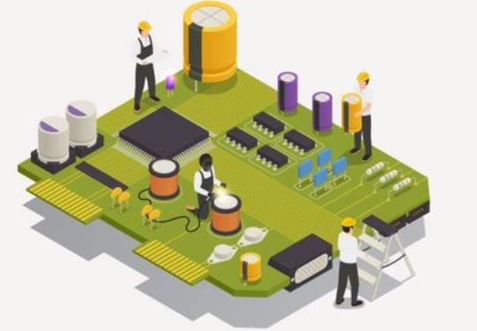
Enclosure for pcb board
Types of enclosure for pcb board
Currently, the most common types of PCB packaging on the market mainly include the following:
1.DIP Packaging
DIP, short for Dual In-line Package is a type of electronic component packaging where the components are inserted into holes on the PCB board through pins or terminals. Dual in-line packaging is primarily used in integrated circuits, converters, computer memory, and microprocessors, and is one of the most common types of PCB packaging.
2.SMD Packaging
SMD, short for Surface Mount Device,is a type of electronic component packaging.Unlike DIP packaging, SMD packaging uses surface mount technology to directly attach electronic components to the PCB board. The benefits of SMD packaging include space saving,performance enhancement, and suitability for mass production. It is an indispensable type of PCB packaging in modern electronic products.
3.BGA Packaging
BGA, short for Ball Grid Array, is a type of electronic component packaging suitable for large-scale integrated circuits, microprocessors, and other high-performance electronic components. In BGA packaging, electronic components are connected to the PCB board through spherical pins and use soldering technology for connection, resulting in stable performance, high reliability, strong heat resistance, and easy maintenance of related circuits.
4.QFN Packaging
QFN, short for Quad Flat No-lead, is a type of electronic component packaging. QFN packaging is a variant of SMD packaging, with the difference being that its pins are located at the bottom or sides of the components. The advantages of QFN packaging include small space occupation, low power consumption, strong electromagnetic interference resistance, and economic practicality.
5.COB Packaging
COB, short for Chip On Board, is a type of packaging for high-precision microelectronic devices. In COB packaging, electronic chips are directly attached to the PCB board, connected to the circuit, and protected with peripheral circuit components and chip dust protection. COB packaging is particularly suitable for high-precision, high-speed processors used in high-end electronic information equipment.
Application:
The choice of PCB packaging depends on specific application scenarios.For example,BGA packaging,with its high pin density and small package size, is particularly suitable for high-performance processors in high-end computers, servers, and mobile devices. QFP packaging is widely used in various consumer electronic products such as televisions,audio systems, and gaming consoles. DIP packaging is more commonly used in industrial control and communication equipment. SMD packaging, with its compact and space-saving characteristics, is widely applied in all kinds of electronic devices.
When performing enclosure for pcb board,certain steps need to be followed.First, choose the appropriate packaging form based on the type and specifications of the electronic components. Then, reserve adequate space on the PCB board to install the packaged electronic components. Next, use soldering, insertion,or crimping methods to fix the electronic components onto the PCB board. Finally, conduct visual inspections and functional tests to ensure the quality of the packaging.
Conclusion
By reading this article, you should have a deeper understanding of enclosure for pcb board By choosing the appropriate packaging method, we can protect electronic components, improve performance and reliability, and help you achieve more circuit design freedom to create higher quality electronic products.