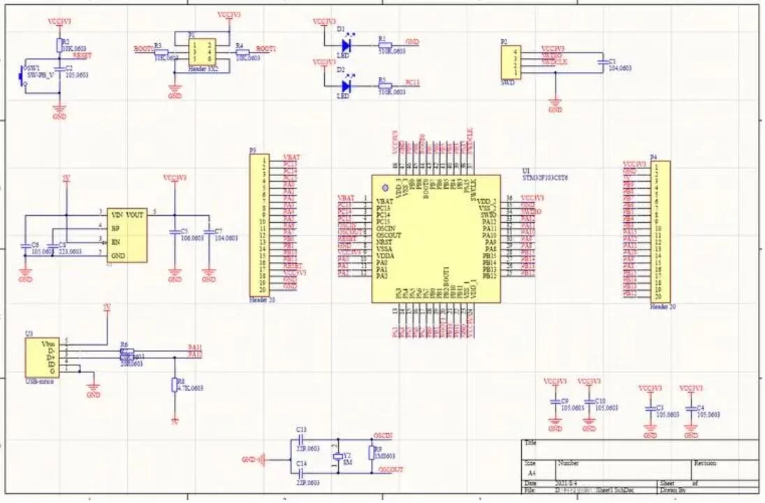
Circuit board drawing, also known as PCB (Printed Circuit Board) design, is a critical step in the development of electronic devices. It involves the creation of schematics and layouts that define the electrical connections and physical arrangement of components on a PCB. This process is essential for ensuring the functionality, manufacturability, and reliability of electronic products. In this article, we will explore the various aspects of PCB drawing, including its importance, tools and design considerations.
Importance of Circuit Board Drawing
PCB drawing is a fundamental aspect of electronic design that bridges the gap between conceptual ideas and physical hardware. A well-drawn circuit board ensures that all components are correctly connected, signals are properly routed, and the board can be manufactured without issues. The quality of the drawing directly impacts the performance, reliability, and cost-effectiveness of the final product. Additionally, a precise and clear drawing aids in troubleshooting, maintenance, and future upgrades of the device.
Tools for Circuit Board Drawing
CAD Software
Computer-Aided Design (CAD) software is the primary tool used for PCB drawing. These software applications provide designers with the ability to create detailed schematics and PCB layouts. Some popular CAD tools include:
Eagle: Known for its user-friendly interface and extensive library of components, Eagle is widely used in both professional and hobbyist circles.
Altium Designer: A comprehensive tool that offers advanced features for high-end PCB design, including 3D modeling and simulation capabilities.
KiCad: An open-source option that provides a powerful suite of tools for schematic capture and PCB layout.
OrCAD: Another professional-grade tool that excels in complex PCB designs and integrates well with other engineering software.
Simulation Software
Simulation software is used to test the electrical behavior of a circuit before it is physically built. These tools help designers identify potential issues and optimize the design for performance and reliability. Examples include:
LTspice: A popular, free SPICE simulation tool that allows for the simulation of analog circuits.
Proteus: A versatile simulation software that supports both analog and digital circuits, often used for embedded systems design.
Multisim: Known for its ease of use and extensive component library, Multisim is widely used in educational settings and by professionals.

Circuit Board Drawing
Design Considerations in Circuit Board Drawing
Component Placement
Component placement is a crucial step in PCB drawing that affects both the electrical performance and manufacturability of the PCB. Key considerations include:
Signal Integrity: Placing components in a manner that minimizes signal degradation and electromagnetic interference.
Thermal Management: Arranging components to ensure efficient heat dissipation and prevent overheating.
Accessibility: Ensuring that components are accessible for assembly, testing, and maintenance.
Routing
Routing refers to the process of creating electrical connections between components using copper traces on the PCB. Effective routing is essential for maintaining signal integrity and minimizing noise. Important aspects of routing include:
Trace Width and Spacing: Determining the appropriate trace width and spacing to handle the required current and prevent short circuits.
Via Usage: Using vias (holes that connect different layers of the PCB) judiciously to maintain signal integrity and minimize manufacturing complexity.
Power and Ground Planes: Implementing solid power and ground planes to provide stable voltage levels and reduce noise.
Design Rules and Constraints
Adhering to design rules and constraints is critical to ensure that the PCB can be manufactured reliably and cost-effectively. These rules may be dictated by the manufacturing process, component specifications, or industry standards. Common design rules include:
Minimum Trace Width: Ensuring that traces are wide enough to carry the required current without overheating.
Clearance: Maintaining adequate spacing between traces to prevent electrical shorts.
Drill Sizes: Specifying appropriate hole sizes for vias and component leads based on manufacturing capabilities.
Circuit board drawing is a critical component of electronic design that requires careful planning, precise execution, and ongoing collaboration. By understanding the importance of this process, utilizing the right tools, adhering to design considerations, and following best practices, designers can create reliable and high-performance PCBs. Ultimately, the success of an electronic product often hinges on the quality of its drawing, making it an essential skill for engineers and technicians alike.