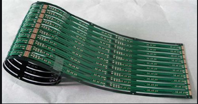
This application note aims to provide PCB design layout guidance for the structure and layout of various PCBs (printed circuit boards) (such as FR4, flexible PCB or ITO panels) used in S-TouchTM capacitive touch sensing PCB design.
Among the PCB substrates currently available on the market, FR4 is the most commonly used one. FR4 is a glass fiber reinforced epoxy resin laminate, and the PCB can be single-layer or multi-layer.
When the size of the touch module is limited, it is not always feasible to use a single-layer PCB, and usually a four-layer or two-layer PCB is used. Take the most commonly used two-layer PCB as an example to introduce PCB layout guidelines.
PCB design and layout
In a two-layer PCB, the S-TouchTM touch controller and other components are laid out on the bottom layer of the PCB, and the sensor electrodes are laid out on the top layer of the PCB.
PCB design rules

Level 1 (top layer)
. The sensor electrode is located on the top layer of the PCB (the upper end of the PCB is fixed with the overlay board). To increase sensitivity, it is recommended to use a sensing electrode with a size of 10 x 10 mm. A smaller size sensing electrode can be used, but the sensitivity will be reduced. At the same time, it is recommended that the size of the sensing electrode does not exceed 15 x 15 mm. If the sensing electrode exceeds this size, it will not only reduce the sensitivity, but also increase the susceptibility to noise.
. The blank area can be filled with grounded copper foil (the trace width is 6 mils, and the grid size is 30 mils).
. The top layer can be used to lay common signal traces (not including sensor signal traces). The sensor signal traces should be laid on the bottom layer as much as possible.
. The distance between the sensing electrode and the grounded copper foil should be at least 0.75 mm. No plug-ins, no viruses
Layer 2 (bottom layer)
. S-TouchTM controller and other passive components should be laid out on the bottom of the PCB design.
. The sensor signal trace will be laid out on the bottom layer. Do not route the sensor signal traces of one channel under the sensing electrodes of other sensing channels.
Sensor signal trace routing method under the touch plate
. The blank area can be filled with grounded copper foil (the trace width is 6 mils, and the grid size is 30 mils).
. The distance between the sensor signal trace and the grounded copper foil should be at least twice the width of the sensor signal trace.
. To reduce crosstalk, the distance between the two sensing electrodes/sensing signal traces should be increased as much as possible. Where possible, add grounded copper foil between the two sensing electrodes/sensing signal traces.
. The length of the sensor signal trace does not need to be exactly the same length. Because of the use of matching tuning capacitors, the input capacitance between the two channels can be balanced. However, when the PCB space permits, it is best to use sensor signal traces of equal length (the size of the sensor electrodes is also uniform). In this way, in order to adjust the sensor capacitive reactance values of all sensing channels to within the dynamic range of the controller sensing, only one standard reference capacitor needs to be set, which simplifies the difficulty of PCB design.
. Any clock, data, or periodic signal traces should not be placed parallel to and adjacent to the sensor signal traces. These signal lines should be as perpendicular as possible to the signal traces of the sensor, or laid out in other areas of the PCB. No plug-ins, no viruses
. If the clock, data or any periodic signal traces do need to be routed in parallel with the signal traces of the sensor, they should be laid out on different layers and cannot overlap, and the length of the parallel part of the signal traces should be shortened as much as possible.
In the previous introduction to the two-layer FR4 PCB, the grounded copper foil was used to fill the blank cross-sectional area of the PCB. The grounding copper foil can help the touch module to shield the external noise source, and can also stabilize the inherent capacitance of the sensor circuit.
However, there are several issues that need to be paid attention to in advance when using grounded copper foil. This is because the grounded copper foil increases the inherent capacitance of the sensor and also increases the possibility of false detection due to water droplets.