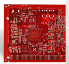
In SMT surface assembly technology, hybrid integrated PCB technology is a new generation of electronic assembly technology developed. The wide application of SMT has promoted the miniaturization and multi-functionalization of electronic products, and has provided conditions for mass production and low defect rate production.
1. PCB and IC baking
1. The PCB has not been more than three months old, and there is no damp, no need to bake. After more than 3 months, the baking time is 4 hours
2. Temperature: 80-100 degrees; IC: BGA package
After 3.1 months, it must be baked for 24 hours in bulk, and at least 8 hours for a new bulk package. If it is an old or disassembled IC, it must be baked for 3 days. Temperature: 100-110 degrees; QFP/SOP/ and other packaged ICs with the original vacuum The packaging does not need to be baked, and the bulk package needs to be baked for at least 8 hours, temperature: 100-110 degrees
Two, PCB patch

1. Solder paste process
2. Red glue process
3. Leaded craft
4. Lead-free process
smt processing flow
3. The type, model, nominal value and polarity of PCB components of each assembly number
To meet the product assembly drawing and schedule or BOM requirements (whether the IC should be burned in), the mounted components should be intact.
Fourth, the solder ends or pins of the mounted components should be immersed in solder paste not less than 1/2 thickness.
For general components, the amount of solder paste extrusion (length) should be less than 0.2mm, and for narrow-pitch components, the amount of solder paste extrusion (length) should be less than 0.1mm.
5. The ends or pins of PCB components are aligned and centered with the land pattern.
Due to the self-positioning effect during reflow soldering, the placement position of the components is allowed to have a certain deviation. The allowable deviation range requirements are as follows:
1. Rectangular component: the solder end width in the width direction of the component is more than 1/2 on the pad; the component solder end and the pad must overlap in the length direction of the component; when there is a rotation deviation, the width of the component solder end is 1/ 2 or more must be on the pad.
2. Small outline transistor (SOT): X, Y, T (rotation angle) deviation is allowed, but the pins (including toe and heel) must all be on the pad.
3. Small outline integrated circuit (SOIC): X, Y, T (rotation angle) are allowed to have mounting deviations, but 3/4 of the device pin width (including toe and heel) must be on the pad.
4. Quad Flat Package Devices and Ultra Small Package Devices (QFP): It is necessary to ensure that 3/4 of the pin width is on the pad, and small mounting deviations of X, Y, and T (rotation angle) are allowed. The toe of the pin is allowed to protrude a little from the pad, but there must be 3/4 of the length of the pin on the PCB pad, and the heel of the pin must also be on the pad.
6. Conventional patch materials must comply with IPC-310 and IPC-610 standards.
Seven, the PCB surface must be clean
There should be no tin beads or tin dross visible in the blood.
8. PCB test range
Check whether the indicator light is on, whether the searcher finds the IP, whether the test image is normal, whether the motor is rotating, test the voice test voice monitoring and intercom, both the machine and the computer must have sound, also provide for mass production and low defect rate production Condition.