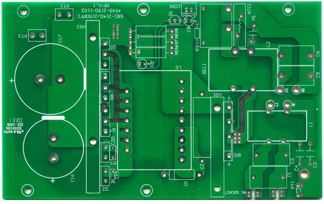
Features of PCB single-sided board:
Single-sided board is on the most basic PCB, the parts are concentrated on one side, and the wires are concentrated on the other side. Because the wires only appear on one side, we call this kind of PCB a single-sided PCB (Single-sided). Because there are many strict restrictions on the design of the single-sided board (because there is only one side, the wiring cannot cross and must go around a separate path), only the early circuits use this type of board; the single-sided wiring diagram is printed by the network (Screen Printing) is the main, that is, the resist is printed on the copper surface, and after etching, the mark is printed with solder mask, and finally the guide hole and shape of the part are completed by punching. In addition, some products that are produced in small quantities and diversified use photoresist to form patterns.
Some basic requirements for PCB circuit board pad design
Pad type
On the printed circuit board, the electrical connections of all components are carried out through pads. The pad is the most important basic unit in PCB design. According to different components and soldering processes, the pads in the printed circuit board can be divided into two types: non-via pads and via pads. Non-via pads are mainly used for soldering surface mount components, and via pads are mainly used for soldering pin-type components.
The choice of pad shape is related to factors such as the shape, size, layout, heating and force direction of the components, and the designer needs to make a selection after comprehensive consideration according to the situation. In most PCB design tools, the system can provide designers with different types of pads such as round pads, rectangular pads and octagonal pads.
1. Round pad
In printed circuit boards, circular pads are the most commonly used pads. For via pads, the main dimensions of the circular pad are the aperture size and the pad size, and there is a proportional relationship between the pad size and the aperture size. For example, the pad size is generally twice the aperture size. Non-via circular pads are mainly used as test pads, positioning pads and reference pads, etc. The main size is the pad size.
2. Rectangular pad

Rectangular pads include square pads and rectangular pads. The square pad is mainly used to identify the first pin used to install components on the printed circuit board. Rectangular pads are mainly used as pin pads for surface mount components. The size of the pad is related to the size of the corresponding component pin, and the pad size of different components is different. For the specific dimensions of some component pads, please refer to section 1.3.
3. Octagonal pad
Octagonal pads are relatively rarely used in printed circuit boards. They are mainly set to meet the requirements of printed circuit board wiring and pad soldering performance at the same time.
4. Shaped pad
In the PCB design process, designers can also adopt some special-shaped pads according to the specific requirements of the design. For example, for some pads with large heat generation, large force, large current, etc., they can be designed into a teardrop shape.
Pad size
The pad size has a great influence on the manufacturability and life of SMT products. There are many factors that affect the size of the pad. When designing the pad size, the range and tolerance of the component size, the need for the size of the solder joint, the accuracy, stability and process capability of the substrate (such as positioning and placement accuracy) should be considered. The size of the pad is specifically determined by factors such as the shape and size of the components, the type and quality of the substrate, the capacity of the assembly equipment, the type and capacity of the process used, and the required quality level or standard.