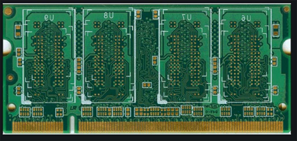
PCB screen printing is a layer of ink traces used to identify PCB components,marks,logos,symbols, etc. If you see, the PCB consists of two parts-components and soldering. In most cases, silk screen is applied to the component part of the PCB.Today,it is also used in welding parts.Screen printing helps manufacturers and engineers to easily identify different parts.

Generally,non-conductive epoxy resin inks are used for pcb screen printing.The formula of this ink is different from ordinary printing inks.In most cases,screen printing uses yellow, white, and black.PCB software screen printing uses certain standard fonts; however,custom fonts can also be used.
What information does pcb screen printing provide?
Silk screen may not have any effect in the function of PCB; however, its value lies in the information it provides. For example, it will help anyone:
Understand the warning symbols
Part polarity
Determine the test point
Locate parts by reference mark
Identifies the unique number of the printed circuit board.
Identify the manufacturer's mark, version number, etc.
Screen printing method
PCB screen printing is applied on PCB in three ways:
1.Manual screen printing:
When the registration tolerance is 0.005" or the line width is greater than 0.007", this is done on the PCB. Manual screen printing is performed using templates containing text and traces. The marks are made of nylon. The ink is guided to the layer or laminate through the template. Next, the ink is cured in an oven. This is one of the easiest ways to create a silk screen layer, and it also supports large text sizes. It may take years to perfect this art.
2.Liquid Photo Imaging (LPI):
This method is used for screen printing lines larger than 4 mil. The LPI process is almost the same as the solder mask application. However, in this method, the laminate is coated with epoxy resin and then placed under ultraviolet light. The board is cured and developed after it. This method ensures higher precision than manual screen printing.
LPI uses white, which requires more ink than the other two screen printing. The setup time for this type of printing is very long.
3.Direct legend printing (DLP):
This is one of the most expensive of the other three processes. In this process, an inkjet projector and acrylic ink were used. Use CAD software to apply ink on the PCB. The ink is then exposed to ultraviolet light. Acrylic links are not suitable for PCBs that may have silver finishes.
Factors to keep in mind when designing pcb screen printing
Do you know that silk screen accounts for 12-15% of the total PCB cost? Text design includes character width, height, thickness, spacing and positioning.The ink cost depends on the screen printing method you choose. Manual screen printing uses epoxy resin ink, and DLP uses acrylic ink. The color and characteristics of the ink are the color influencing factors.
The following are some things to consider when designing a PCB with silk screen legends.
Therefore, when choosing screen printing for PCBs,it is important to make the right choice.
The silk screen must be limited to one side as much as possible. This cuts costs in half. Many PCB assembly services charge a fee for double-sided PCB printing.
Use standard colors and large shapes to make the silk screen stand out. You can also check whether the manufacturer provides any special types of ink.
Direct Legend Printing (DLP) and Liquid Photo Imaging (LPI) are more expensive than other equipment because their setup requires higher investment.