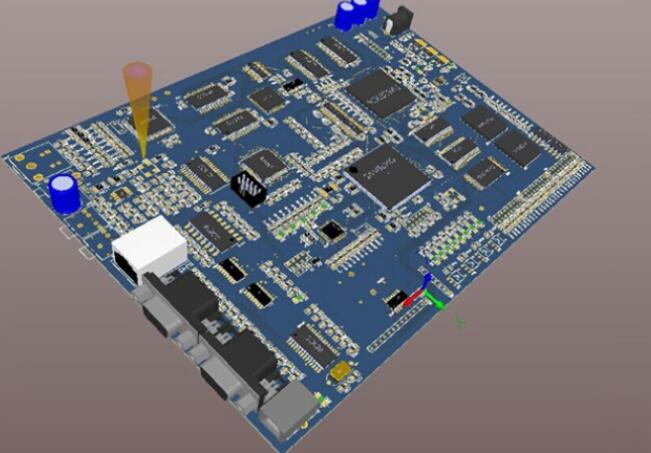
Via (Via), also known as metalized holes, is one of the important elements of PCB design. In double-sided and multi-layer boards, in order to connect the printed wires between the layers, a common hole, that is, a via hole, is drilled at the intersection of the wires that need to be connected in each layer. There are three types of vias, namely blind vias, buried vias, and through vias. In this article, Banermei has collected some classic questions and answers related to PCB "vias", I hope it will be helpful to everyone.
1. I often see many holes on the PCB board. Is there more of these vias, the better? Are there any rules?
Answer: No. The use of vias should be minimized, and when vias have to be used, it is also necessary to consider reducing the impact of vias on the circuit.
2. In the layout of the board, if the wires are dense, there may be more vias. Of course, it will affect the electrical performance of the board. How can I improve the electrical performance of the board?
Answer: For low-frequency signals, vias do not matter. For high-frequency signals, reduce vias as much as possible. If there are many lines, consider multi-layer boards.

3. How much influence does the through hole and blind hole have on the signal difference? What are the principles applied?
Answer: The use of blind vias or buried vias is an effective method to increase the density of multilayer boards, reduce the number of layers and board size, and greatly reduce the number of plated through holes. However, in comparison, through holes are easy to implement in process and low cost, so through holes are generally used in the design.
4. Can you explain the relationship between the line width and the size of the matching via?
Answer: It is difficult to say that there is a simple proportional relationship, because the simulations of the two are different. One is surface transmission and the other is ring transmission. You can find a via hole impedance calculation software on the Internet, and then keep the impedance of the via hole consistent with the impedance of the transmission line.
5. What is the relationship between the line width and the size of the vias on the PCB board and the magnitude of the current passing through?
Answer: The thickness of the general PCB copper foil is 1 ounce, about 1.4 mils, and the maximum current allowed for roughly 1 mil line width is 1A. The via hole is more complicated. In addition to the size of the via pad, it is also related to the thickness of the hole wall sinking copper after electroplating during the processing.
6, Sqrt(L/C) should be matched with via holes according to requirements?
Answer: Yes, it means impedance matching. Adjust the parameters of the vias to achieve a better impedance smooth transition.
7. Is there a corresponding relationship between temperature change and via impedance?
Answer: The temperature change mainly affects the reliability of the vias. The material selection needs to consider the CTE value of the material.
8. How to deal with the avoidance of vias in the wiring process for high-speed PCBs? What are some good suggestions?
Answer: For high-speed PCBs, it is best to punch fewer vias, and increase the signal layer to solve the need to increase vias.
9. What is the function and principle of adding ground vias near the trace vias?
Answer: PCB vias are classified according to their functions and can be divided into the following types:
1) Signal vias (via structure requirements have the least impact on the signal)
2) Power and ground vias (via structure requires the smallest distributed inductance of vias)
3) Thermal vias (via structure requires the minimum thermal resistance of vias)
The vias mentioned above are grounded vias. The effect of adding a grounded via near the trace via is to provide the shortest return path for the signal.
Note: The via hole for signal change layer is a discontinuity point of impedance, and the return path of the signal will be disconnected from here. In order to reduce the area surrounded by the return path of the signal, some grounding must be punched around the signal via hole. The hole provides the shortest signal return path and reduces the EMI radiation of the signal. This radiation will increase significantly as the frequency of the signal increases.
10. When the signal via hole diameter is relatively small (for example, 0.3mm diameter), will the via metallization be insufficient in this case?
Answer: If the aperture is small and deep (that is, the aperture is relatively large), it may not be completely metalized.