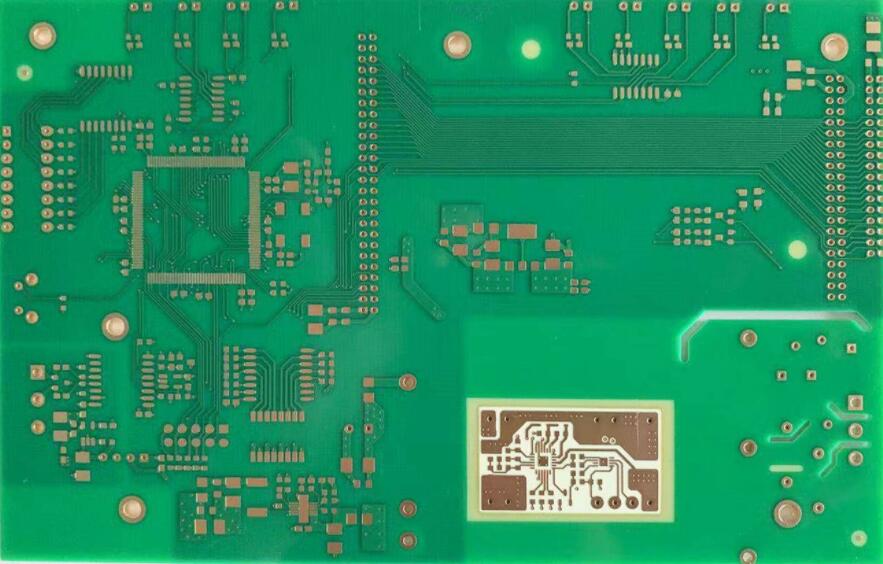
PCB production engineers repeat the work of pulling wires with thousands of wires and various packages on the board every day. Perhaps many people will find it very boring and boring. It looks like a software operation porter. In fact, designers have to make trade-offs between various design rules in the process, taking into account performance, cost, craftsmanship and other aspects, and pay attention to the reasonable and neat layout of the board, which is not as good as it seems. Simplicity requires more wisdom. Good working habits will benefit you a lot, making your design more reasonable, production easier, and better performance.
(1) Details determine success or failure
PCB design is a meticulous work, all it takes is carefulness and patience. The mistakes often made by newbies who are just starting to design are detailed errors. The device pin is wrong, the device package is used wrong, the pin sequence is reversed, etc. Some can be solved by flying leads, and some may make a board directly become a waste. When drawing the package, check it again and compare it with the actual device before printing the package. Take a look at it. Checking it again is not obsessive-compulsive disorder. It is just to avoid these low-level mistakes that are easy to make as much as possible. Otherwise, no matter how good the design is, the board is covered with flying lines, and it is far from excellent.

(2) Learn to set rules
In fact, not only advanced PCB design software needs to set wiring rules, some simple and easy-to-use PCB tools can also set rules. After all, the human brain is not a machine, so it is inevitable that there will be negligence and mistakes. So set some easily overlooked problems into the rules, let the computer help us to check, try to avoid making some low-level mistakes. In addition, a complete rule setting can better regulate the subsequent work. The so-called sharpening of the knife does not accidentally chop wood, the more complex the scale of the board, the more important the rule setting becomes. Nowadays, many EDA tools have automatic wiring function. If the rules are set in sufficient detail, let the tools design it for you. Wouldn't it be more pleasant for you to have a cup of coffee by the side?
(3) The more you think about others, the less your own work
When doing PCB design, try to consider the needs of some end users as much as possible. For example, if you are designing a development board, you should consider placing more silk screen information when designing the PCB, so that it will be more convenient when you use it, and it will not be used to retrieve the schematic diagram or seek the support of the designer. If the design is a mass production product, then more consideration should be given to the problems encountered on the production line. Devices of the same type should have the same direction as possible, whether the device spacing is appropriate, the process edge width of the board, and so on. The earlier these issues are considered, the less they will affect the subsequent design, and the workload of subsequent support and the number of board changes can also be reduced. It seems that the time it takes to start the design has increased, but in fact it has reduced the amount of follow-up work. When the board space signal permits, try to place more test points to improve the testability of the board, so that it can also save more time in the subsequent debugging stage and provide more ideas for finding problems.
(4) Draw the schematic diagram
Many engineers think that the layout work is more important. The schematic diagram is to generate a netlist to facilitate PCB inspection. In fact, the role of the schematic diagram will be greater in the subsequent circuit debugging process. Whether it is to find problems or communicate with colleagues, or the schematic diagram is more intuitive and convenient. In addition, develop the habit of labeling in the schematic diagram, and mark the problems that should be noticed during the layout of each part of the circuit on the schematic diagram, which is a good reminder for yourself or for others. Hierarchical schematic diagram, divide the circuit of different functions and different modules into different pages, so that whether it is to read the diagram or reuse it in the future, the workload can be significantly reduced. Using a mature design is always less risky than designing a new circuit. Every time I see all the circuits on a drawing, a densely packed device, my head can be bigger.
(5) Properly lay out the circuit
After the impatient engineer finished drawing the schematic and imported the netlist into the PCB, he couldn't wait to put the device in place and start pulling the wire. In fact, a good PCB layout can make your wire-drawing work easier and make your PCB work better. Each board will have a signal path, and the PCB layout should follow this signal path as much as possible so that the signal can be transmitted smoothly on the board. People don't like to walk through the maze, and the signal is the same. If the schematic diagram is designed according to the module, the PCB is the same. According to different functional modules, the board can be divided into several areas. Separate analog and digital, separate power supply signals, separate heating devices and susceptible devices, do not place larger devices too close to the edge of the board, pay attention to the shielding of radio frequency signals, etc.... Spend a little more time to optimize the PCB layout, you can Save more time when pulling the string.