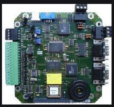
Today’s telling PCB design has more and more stringent requirements for the layout. The layout basically determines the general direction and structure of the wiring, the division of power and ground planes, and the control of noise and EMI. Therefore, the performance of the PCB design is good or bad. Much depends on whether the layout is reasonable.
Engineers often spend a lot of time and energy on layout. Pre-layout-pre-simulation-relayout-optimization. These processes account for about 50% or even more of the entire project design time.
The following summarizes a general layout steps and rules for reference only.
Many other issues should be considered in the actual circuit design, such as heat dissipation, mechanical performance, and the placement of some special circuits. The specific layout criteria are determined by the actual application.
The layout must first start with understanding the schematic diagram of the system circuit. It is necessary to divide the digital, analog, and mixed digital/analog components in each circuit (check the chip information), and pay attention to the positioning of the power and signal pins of each IC chip.
According to the proportion of each part of the circuit, the wiring area of the digital circuit and the analog circuit on the PCB is preliminarily divided, and the digital components, analog components and their corresponding wiring are as far away as possible and limited to their respective wiring areas. After the area is divided, the components can be placed. The general order is hybrid components-analog components-digital components-bypass capacitors.
Digital-analog hybrid components must be placed at the junction of the digital signal area and the analog signal area, and pay attention to the correct direction, that is, the digital signal and analog signal pins face their respective wiring areas; pure digital or analog components must be placed Within their respective specified ranges; the crystal oscillator circuit should be as close as possible to its driving device.
Noise-sensitive devices should be kept away from high-frequency signal wiring. At the same time, noise-sensitive signals such as the reference voltage Uref should also be kept away from components that are prone to high noise.
In general, digital components are placed together as much as possible to reduce the line length and reduce noise. However, if it is a signal wiring with timing requirements, the layout needs to be adjusted according to the line length and structure, which should be determined by simulation. The bypass capacitor needs to be placed as close as possible to the power supply pins of the chip, especially high-frequency capacitors. A large-capacity (such as 47uF) capacitor can be placed near the power interface to keep the power supply stable and reduce low-frequency noise interference.

How to improve the quality of BGA welding
With the development of light, thin and short products, the welding accuracy of circuit boards (especially soft boards and PCB thin boards) is getting higher and higher, mainly reflected in the smaller and smaller part pitch PITCH, so that the control requirements for the welding process are increasing. The higher the value, one of which is reflected in the flatness of the board placement when printing.
Both the soft board and the thin board have one thing in common, that is, the board is relatively soft. It is fixed on the carrier in the traditional way (fixed with single-sided PI tape), so that the board will not be tightly integrated with the carrier. There will be a shape change, which will cause a problem of hitting.
Another fixing method is to coat the carrier with a layer of silica gel. Although this method can solve the problem of tight bonding between the board and the carrier and no deformation during the printing, it will bring another problem:
1. The thickness uniformity of silica gel coating is not easy to control each time
2. Silica gel is easy to remain and does not meet environmental protection requirements
3. Silica gel is not easy to maintain, has a short life and high cost
4. Silica gel is not easy to remove after use
Recently, a Teflon double-sided adhesive has been developed, which can completely replace the traditional way of coating silicone and meet ROHS requirements. The test results of many PCB manufacturers have shown that the welding yield has been improved (the higher the accuracy requirement, the higher the yield The higher the ratio)