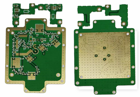
1. Layout
10 rules of component layout:
1. Follow the layout principle of "big first, then small, difficult first, easy first", that is, important unit circuits and core components should be laid out first.
2. The principle block diagram should be referred to in the PCB layout design, and the main components should be arranged according to the main signal flow law of the single board.
3. The arrangement of components should be convenient for debugging and maintenance, that is, large components cannot be placed around small components, components that need to be debugged, and there must be enough space around the components.
4. For the circuit parts of the same structure, use the "symmetrical" standard layout as much as possible;
5. Optimize the layout according to the standards of uniform distribution, balanced center of gravity, and beautiful layout;
6. The same type of plug-in components should be placed in one direction in the X or Y direction. The same type of polarized discrete components should also strive to be consistent in the X or Y direction to facilitate production and inspection.
7. The heating elements should generally be evenly distributed to facilitate the heat dissipation of the veneer and the whole machine. Temperature sensitive devices other than the temperature detection element should be kept away from the components that generate large amounts of heat.
8. The layout should meet the following requirements as far as possible: the total connection is as short as possible, and the key signal line is the shortest; high voltage, large current signal and low current, low voltage weak signal are completely separated; analog signal and digital signal are separated; high frequency signal Separate from low-frequency signals; the spacing of high-frequency components should be sufficient.

9. The layout of the decoupling capacitor should be as close as possible to the power supply pin of the IC, and the loop formed between it and the power supply and ground should be the shortest.
10. In the component layout, appropriate consideration should be given to putting the devices using the same power supply together as much as possible to facilitate future power supply separation.
2. Right-angle routing
Right-angle wiring is generally a situation that needs to be avoided as much as possible in PCB wiring, and it has almost become one of the standards for measuring the quality of wiring. So how much influence will the right-angle wiring have on signal transmission? In principle, right-angle routing will change the line width of the transmission line, causing discontinuity in impedance. In fact, not only right-angle routing, but also corners and acute-angle routing may cause impedance changes.
The influence of right-angle routing on the signal is mainly reflected in three aspects:
One is that the corner can be equivalent to a capacitive load on the transmission line, which slows down the rise time;
Second, discontinuous impedance will cause signal reflection;
The third is the EMI generated by the right-angle tip.
3. Differential wiring
Differential signal (Differential Signal) is more and more widely used in high-speed circuit design. The most critical signal in the circuit is often designed with a differential structure. Definition: In layman's terms, the driver sends two equal and opposite phases. Signal, the receiving end judges the logic state "0" or "1" by comparing the difference between the two voltages. The pair of traces carrying differential signals is called differential traces.
Compared with ordinary single-ended signal traces, differential signals have the most obvious advantages in the following three aspects:
a. Strong anti-interference ability, because the coupling between the two differential traces is very good. When there is noise interference from the outside, they are almost coupled to the two lines at the same time, and the receiving end only cares about the difference between the two signals. Therefore, the external common mode noise can be completely canceled.
b. It can effectively suppress EMI. For the same reason, due to the opposite polarity of the two signals, the electromagnetic fields radiated by them can cancel each other out. The tighter the coupling, the less electromagnetic energy vented to the outside world.
c. The timing positioning is accurate. Because the switch change of the differential signal is located at the intersection of the two signals, unlike ordinary single-ended signals, which rely on the high and low threshold voltages to determine, it is less affected by the process and temperature, which can reduce the error in the timing., But also more suitable for low-amplitude signal circuits. The current popular LVDS (low voltage differential signaling) refers to this small amplitude differential signaling technology.
For PCB engineers, the most concern is how to ensure that these advantages of differential wiring can be fully utilized in actual wiring. Perhaps anyone who has been in touch with Layout will understand the general requirements of differential wiring, that is, "equal length and equal distance".
The equal length is to ensure that the two differential signals maintain opposite polarities at all times and reduce the common mode component; the equal distance is mainly to ensure that the differential impedances of the two are consistent and reduce reflections. "As close as possible" is sometimes one of the requirements of differential wiring.
4.Snake line:
Snake line is a type of routing method often used in PCBLayout. Its main purpose is to adjust the delay to meet the system timing design requirements. The designer must first have this understanding: the serpentine line will destroy the signal quality, change the transmission delay, and try to avoid using it when wiring. However, in actual design, in order to ensure that the signal has sufficient hold time, or to reduce the time offset between the same group of signals, it is often necessary to deliberately wind the wire.