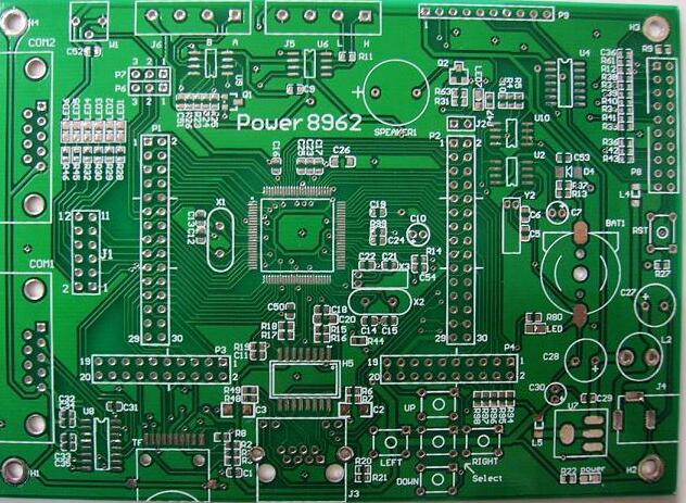
Vias play an important role in the design of Printed Circuit Boards,however,their accompanying parasitic capacitance and parasitic inductance pose a potential challenge that can significantly affect the overall performance of the circuit. Especially in high-speed circuit design,these parasitic effects should not be underestimated as they can lead to increased signal transmission delays and significant degradation of signal quality.
Parasitic characteristics of vias mainly include parasitic capacitance and parasitic inductance.The parasitic capacitance of an via is the capacitance between the via and the surrounding ground, which may not be significant at relatively low frequencies, but should not be underestimated for high-speed circuits. In addition, parasitic inductance mainly originates from the structure and layout of the vias, especially in the case of long signal lines, the effect of parasitic inductance will be more obvious.
In high-speed circuit design, the parasitic capacitance and parasitic inductance of the vias significantly affect the signal transmission performance. Parasitic capacitance mainly leads to longer signal rise times, which reduces the circuit's operating speed, while parasitic inductance may weaken the effectiveness of bypass circuits, further affecting the power system's filtering function.
The main effect that the presence of parasitic capacitance in an over-hole can have on a circuit is to lengthen the rise time of the signal, reducing the speed of the circuit. In high-speed digital circuits, this delay is more pronounced as the signal frequency rises (above 1 GHz),thus affecting the overall circuit performance. The parasitic capacitance of an overbore is more than a simple electrical characteristic; its presence causes the signal to be delayed before it reaches the target component, and therefore requires special attention from the designer.

Parasitic inductance is often considered to have a more serious effect on a circuit than parasitic capacitance. Parasitic inductance in an overbore can weaken the bypass capacitors and diminish the filtering benefits of the entire power system. This inductance can cause phase interference and amplitude degradation of signals, especially at high speed signal transmission. Careful consideration needs to be given to the length and structure of the vias to reduce the negative effects of parasitic inductance.
According to the test results, signals are significantly delayed when passing through both the vias and the no-vias cases. For example,the time required for the signal to travel to the next test point is 458 ps in the case of no vias, compared to 480 ps with vias,a delay of 22 ps, which is a direct indication of the parasitic effect of vias.The rise time variation caused by the parasitic capacitance of the vias has been quantified, suggesting that the designer needs to control and optimise it in the high-speed PCB layout.
Parasitic capacitance and inductance of vias are critical factors that cannot be ignored in high-speed circuit design. Proper design and layout can significantly improve signal quality and ensure stable circuit operation. In the future design process, it is important to continue to study the impact of these parasitic parameters and their optimisation countermeasures in depth, in order to continuously improve the overall capability of high-speed PCB design.