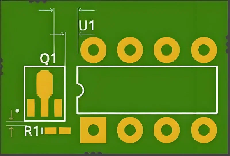
Silk to solder mask clearance is crucial in PCB design, affecting the readability, manufacturability and overall quality of the board. Silkscreen is a mark printed on the surface of the PCB to mark component locations, test points or brand information, while the solder mask covers the bare copper of the PCB to prevent soldering shorts and corrosion. If the spacing between the silkscreen and the solder mask is unreasonable, the silkscreen may be covered by solder, affecting identification, and even causing production defects. Therefore, in PCB design, it is crucial to strictly adhere to the spacing requirements between the silkscreen and the solder mask.
Silk to solder mask clearance is mainly set according to the PCB manufacturing process.
Different factories may have different standards, but in general, the recommended minimum spacing is 0.15mm (6mil) to ensure that the silkscreen does not cover the pads or solder joints. In addition, the following points need special attention:
Avoid silkscreen pressing the pad: The silkscreen layer should not cover the pad, otherwise during the soldering process, the silkscreen ink may affect the soldering quality and even cause soldering failure.
Keep a reasonable distance from the edge of the pad: Generally speaking, the silk screen should be kept at a distance of more than 0.2mm from the edge of the pad to reduce errors in the manufacturing process.
Prevent silk screen diffusion: Silk screen ink may diffuse during the production process, so it is necessary to consider the production tolerance and avoid being too close to the pad during design.
Minimum requirements for silk screen fonts: It is generally recommended that the silk screen font height be at least 1mm and the line width be at least 0.15mm to ensure clear readability during PCB manufacturing.

Silk to solder mask clearance
Irrational design of silk to solder mask clearance may cause the following problems:
Poor soldering: If the silk screen covers the pad, it may affect the soldering effect, resulting in false soldering or poor solder joint connection.
Difficult identification: If the silk screen is too close to the pad or component, it will be covered by solder after soldering, affecting subsequent repairs or testing.
Production error: Since the silk screen ink may have alignment errors or diffusion during printing, too small a spacing will increase the difficulty of production and increase the defective rate of finished products.
Pad contamination: Silk screen ink may affect the wettability of the solder, resulting in reduced solder joint reliability.
Silk screen to solder mask gap optimization mainly includes the following aspects:
Reasonable layout of silk screen: During the PCB design stage, ensure that the silk screen is away from the pad and soldering area to reduce the impact of production errors.
Use professional design software to check: PCB design software such as Altium Designer,Eagle, etc. all provide inspection functions for silk screen layer and solder mask layer, which can automatically detect whether the spacing meets the standard during design. Communicate with PCB manufacturers: Different PCB manufacturers have different process capabilities. It is best to confirm the manufacturer's minimum silk screen spacing requirements before designing and optimize accordingly.Silk screen color and readability: Silk screen is usually white or yellow, but it is necessary to ensure that there is enough contrast with the PCB background color to improve readability.
Silk to solder mask clearance may have different requirements in different types of PCBs. For example:
Single-sided board and double-sided board: Usually a regular spacing (0.15mm~0.2mm) is used, and silk screen is mainly used to mark component information.
HDI PCB: Due to the dense pads, the silk screen spacing requirements are more stringent, and may need to be increased to more than 0.2mm, and a more sophisticated silk screen process is used.
FPC: Due to the soft substrate, the silk screen ink is easy to spread, so the distance between the silk screen and the solder mask is usually appropriately increased.
Automotive electronics and industrial control boards: High reliability requirements, so the silk screen layout is more standardized and the spacing requirements are more stringent.
With the development of PCB manufacturing technology, Silk screen to solder mask gap is also being optimized. Future trends include:
Laser silk screen technology: Compared with traditional silk screen printing, laser silk screen printing can achieve finer markings and improve the spacing accuracy between silk screen and pads. AOI: In the PCB production process, AOI is used to detect whether the spacing between silk screen and pad meets the design requirements and improve the yield rate.Environmentally friendly silk screen ink: Use new environmentally friendly silk screen ink to improve temperature resistance and anti-diffusion ability, and reduce the impact on the welding process.Intelligent PCB design optimization: AI-assisted PCB design software can automatically optimize the silk screen layout and improve the rationality of the silk screen and solder mask clearance.
Silk to solder mask clearance is an important parameter that cannot be ignored in PCB design. Reasonable spacing design not only helps to improve the manufacturability of PCB, but also reduces production defects and improves the reliability of circuit boards. With the continuous development of the electronics manufacturing industry, silk screen technology is also constantly improving, providing more accurate and efficient solutions for the PCB industry. Therefore, when designing PCBs, engineers should fully consider the spacing requirements between silk screen and solder mask to ensure that the design meets manufacturing standards and ultimately produce high-quality electronic products.