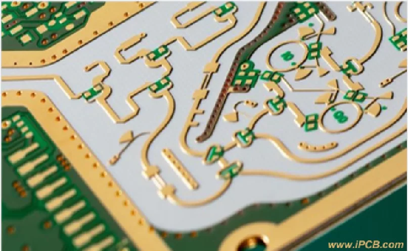
RF PCB layout plays an essential role in modern electronic equipment. The radio frequency circuit has the characteristics of high frequency, high sensitivity and low noise. A good RF PCB layout can reduce the reflection and loss of the signal, reduce electromagnetic interference, and improve the reliability and stability of the system.
Basic principles of RF PCB layout
1. Impedance matching
Impedance matching is one of the basic principles of RF printed circuits design. In radio frequency circuits, the transmission of signals must maintain a certain impedance to ensure the integrity of the signal and the efficiency of the transmission. The impedance does not match, this will lead to reflection and loss of the signal, which will affect its performance. system. It is necessary to select the appropriate impedance value according to the signal frequency and the characteristics of the transmission line, and realize the impedance matching with a reasonable layout design. Common impedance matching methods include micro strip line matching, coplanar waveguide matching, decoupling, etc. Can be found.
2. Signal isolation:
(1) Place different signals in layers to avoid cross-decoupling interference between signals.
(2) Use a screen or protective layer to isolate sensitive signals from other signals.
(3) Reasonably organize the grounding method to reduce the interference of the grounding current on the signal.
3. Power supply and grounding design:
(1) Select a suitable power filter to reduce the interference of power noise in the radio frequency signal.
(2) Decently organize the layout of the power supply and the ground to avoid loop interference between the power supply and the ground.
(3) Use a large ground plane area to improve the stability and reliability of grounding.

RF PCB layout
Special design stages of RF PCB layout
1. The circuit design is carried out first, and the circuit design consists of two stages: schematic design and layout of the printed circuit board design. In at the schematic design stage, it is necessary to select the appropriate electronic components according to the functional requirements of the system and design a reasonable circuit diagram diagram. In The stage of designing the layout of the printed circuit board requires rational placement of electronic components on the printed circuit board in accordance with the schematic diagram of the circuit, and the design of the wiring must be carried out.
2. Basic components such as component placement devices are placed as close as possible to reduce the transmission path and signal loss.
(2) Impedance matching: According to the impedance matching requirements, the position and direction of the components are reasonably arranged to ensure the impedance matching.
(3) Signal Isolation: Keep the different signal sources and sensitive components such as amplifiers as decoupled as possible to reduce interference between signals.
(4) Heat dissipation problems: For high-power components, heat dissipation problems should be taken into account, and the location and arrangement of components should be organized rationally to improve the heat dissipation effect.
3. Wiring design
(1) Impedance matching: According to the impedance matching requirements, select the appropriate and suitable cable width to achieve impedance matching.
(2) Signal isolation: Place the different signal cables as far apart as possible to avoid cross-decoupling interference between the signals.
(3) Grounding design: reasonable arrangement of grounding cables to reduce the interference of grounding current on the signal.
(4) Electromagnetic interference: prevent the formation of loops in the wiring and reduce electromagnetic interference.
4.Electromagnetic protection design
The following methods can be used when designing an electromagnetic shield:
(1) Use a protective cover or protective layer: cover the sensitive components or the entire radio frequency circuit with a protective cover or protective layer to reduce external electromagnetic interference.
(2) Reasonable regulation of grounding methods: ground the protective cover or protective layer to improve the protective effect.
(3) Use filters: Use filters on the signal input and output ports to reduce the input of external electromagnetic interference.
Precautions for the arrangement of RF PCB layout
1. Right-angled turns should be avoided as much as possible. Turning at a right angle causes reflection and loss of the signal, which will affect the performance of the system. Curved turns or 45-degree turns can be used to reduce reflection and signal loss.
2. The length of the cables should be controlled as much as possible. Too long wiring affects the performance of the system, resulting in a delay and loss of signal transmission. A short and straight wiring method can be used to reduce the transmission delay and signal loss.
3. Parallel wiring should be avoided as much as possible. Parallel wiring can cause decoupling between signals and affect system performance. Cross or vertical wiring can be used to reduce decoupling interference between signals.
4.Particular attention should be paid to the direction of placement of the components. Amplifiers, filters, etc. For some sensitive components, such as., the direction of the input and output ports should be as consistent as possible with the signal transmission direction to reduce the reflection and loss of the signal.
5.Simulations and tests must be carried out to verify the accuracy and performance of the design. You can use professional radio frequency simulation software for simulation analysis such as ADS, HFSS, etc. At the same time, S-parameter tests, noise shape tests, etc. Like real tests., can also be carried out to ensure that the performance of the design meets the requirements.
In short, the RF PCB layout plays an essential role in modern electronic equipment. Thanks to the reasonable layout design, the quality and stability of the radio frequency signals can be improved, the noise interference can be reduced, and the reliability and stability of the system can be improved. improved. In the future, the design of electronic equipment, the layout of RF printed circuit boards will continue to play an important role, ensuring the high performance and high reliability of electronic equipment.