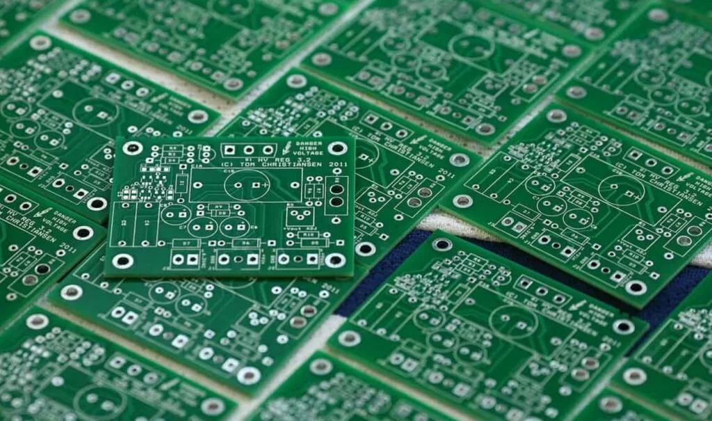
PWB Printed Wiring Board is an essential component in almost every electronic device you can imagine. From consumer electronics like smartphones and laptops to industrial machinery and even medical devices, PWBs are fundamental to ensuring smooth and efficient operation. In this article, we will delve into the world of PWBs, exploring their design, production, and the vital role they play in modern electronics.
PWB Printed Wiring Board is a technology that has evolved significantly over the years, adapting to new demands for smaller, more efficient, and more complex devices. These boards are used to mechanically support and electrically connect electronic components using conductive pathways, tracks, or signal traces etched from copper sheets laminated onto a non-conductive substrate. The intricate process of designing and manufacturing PWBs is crucial for ensuring optimal performance in any device that uses them.PWB production starts with design. Engineers must carefully layout the electronic circuits, taking into account both the electrical and mechanical aspects. This process is more complex than it sounds; engineers need to ensure that the routing of the circuits is both functional and efficient. Advanced computer-aided design (CAD) tools are employed at this stage to help optimize the design, simulate the circuit's behavior, and ensure the final product will work as intended.

PWB Printed Wiring Board
In terms of materials, the PWB typically consists of a substrate, often made of fiberglass-reinforced epoxy resin, which provides mechanical support and insulation. On top of this, a layer of copper is added to form the electrical pathways that connect different components. Depending on the complexity of the design, the PWB can have multiple layers, with conductive traces on each one, allowing for intricate and compact circuit designs.Once the design is complete, the PWB moves to the production stage, which involves a number of complex steps. The copper layer on the substrate is etched to create the circuit pattern. This is done by applying a protective mask to the areas that need to remain conductive, then using a chemical etching solution to remove the unwanted copper. After this, holes are drilled into the board to allow for component mounting and interconnection between layers.Next comes the plating process, where the drilled holes are lined with copper to ensure a strong electrical connection between the layers. This is followed by a solder mask application, which protects the copper traces and helps prevent short circuits. Finally, a surface finish is applied to the areas where components will be soldered, ensuring a strong and reliable connection.
PWB Printed Wiring Board manufacturing is not only about making connections. It is also about ensuring the durability and longevity of the product. The boards must be able to withstand mechanical stress, heat, and other environmental factors without degrading or losing functionality. This is why selecting the right materials and following stringent manufacturing processes are so important.Moreover, the rise of 5G technology, artificial intelligence, and the Internet of Things (IoT) is creating new challenges and opportunities for PWB manufacturers. As these technologies continue to evolve, there will be an increasing need for PWBs that can handle higher frequencies, faster data transfer rates, and more complex circuitry. This means that the materials and processes used to make PWBs will need to keep pace with these advancements.
One of the biggest trends in PWB Printed Wiring Boardmanufacturing is the shift towards more environmentally friendly production methods. As the world becomes more conscious of its environmental impact, manufacturers are working to reduce the use of harmful chemicals and materials in the production process. Lead-free solder, for example, has become the industry standard in many parts of the world. Additionally, manufacturers are exploring the use of recyclable and biodegradable materials in their products, further reducing the environmental footprint of electronic devices.In terms of applications, PWBs are used across a wide range of industries. In the automotive sector, for example, PWBs are used in everything from engine control units to infotainment systems. In the medical field, they are found in devices like pacemakers, diagnostic equipment, and monitoring systems. In telecommunications, PWBs form the backbone of the infrastructure that supports our modern communication networks, from base stations to satellites.
The future of PWB technology looks bright. As electronic devices become more advanced, the demand for smaller, faster, and more reliable PWBs will continue to grow. Manufacturers are investing heavily in research and development to stay ahead of the curve, developing new materials and processes that will enable them to produce even more sophisticated boards.One area that holds particular promise is the use of nanotechnology in PWB manufacturing. By incorporating nanoscale materials into the production process, manufacturers could create boards that are smaller, lighter, and more efficient than ever before. This could open up new possibilities for device design, allowing for the creation of even more compact and powerful electronic products.
In conclusion, PWB Printed Wiring Board technology is essential to the functioning of modern electronics. From the design and manufacturing process to its wide range of applications, PWBs play a crucial role in ensuring the efficiency and reliability of electronic devices. As technology evolves, PWBs will continue to advance, providing even greater functionality and performance in the years to come.