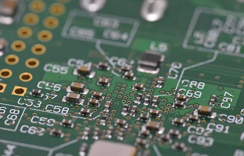

Earthing layers play a crucial role in PCB design and production. Ground Plane not only aid in stable signal transmission but also effectively reduce electromagnetic interference and noise. This article will delve into the application and importance of ground Plane in PCB design and production.
Firstly, ground Plane refer to the conductive layers dedicated to grounding in a PCB. These layers usually cover an entire layer of the circuit board and connect to all the ground lines in the circuit, forming a complete grounding system. The presence of ground Plane can significantly reduce noise and electromagnetic interference in the circuit, thus improving the stability and reliability of the circuit. In the design process, choosing the appropriate layout and configuration of ground Plane is crucial, especially in high-frequency circuits and complex systems.
Earthing layers play an indispensable role in high-frequency circuit design,. High-frequency signal transmission is prone to electromagnetic interference and reflection, leading to signal distortion and performance degradation. By setting up ground Plane, a low-impedance return path can be formed, reducing signal reflection and interference, ensuring signal integrity and stability. Additionally, ground Plane can serve as shielding layers, isolating interference between different signals and enhancing the circuit's anti-interference capability.

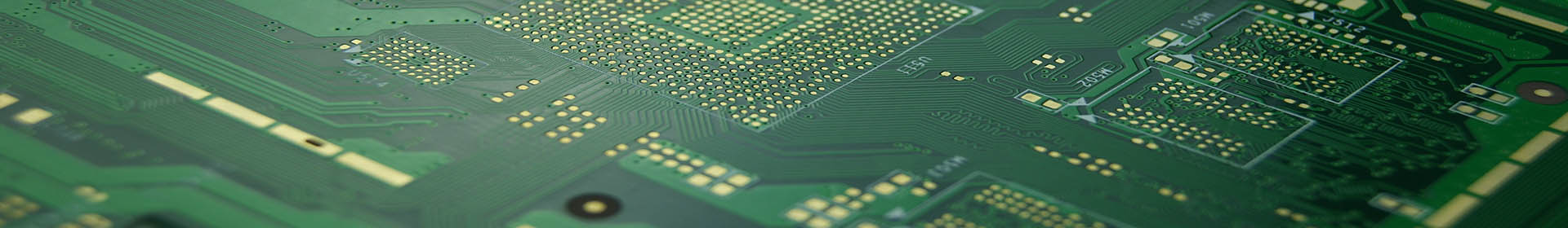
Earthing layers
Ground Plane are equally important in power management. In multilayer PCB design, independent power and ground Plane are often set up to achieve better power distribution and management. The ground Plane, closely coupled with the power layers, form a low-impedance power network, providing stable power supply and reducing power noise and interference. Especially in high-power and high-current applications, the design and layout of ground Plane are critical for power stability and efficiency.
Earthing layers also requires special attention in actual manufacturing process. Typically, ground Plane use thick copper foil materials to enhance their conductivity and heat dissipation capabilities. Moreover, it is essential to ensure insulation and separation between the ground Plane and other layers to avoid accidental short circuits and interference. In multilayer PCBs, ground Plane are usually stacked with signal layers, power layers, and other layers to form a complete multilayer structure. During production, precise control of the alignment and bonding between layers is necessary to ensure the continuity and integrity of the ground Plane.
Beyond basic electrical characteristics, ground Plane also play a key role in the safety and reliability of electronic products. By providing a stable ground reference, ground Plane prevent damage to the circuit from electrostatic discharge and electrical overloads. Additionally, in some high-voltage and high-power applications, ground Plane can serve as safety grounding paths, protecting users and equipment. Through proper design of ground Plane, the safety and reliability of electronic products can be significantly enhanced, extending their lifespan.
The implementation of earthing layers can aid in the mitigation of common-mode noise in differential signal pairs. In high-speed digital circuits, differential signaling is often used to improve signal integrity and reduce electromagnetic interference (EMI). However, common-mode noise, which affects both lines of a differential pair equally, can still degrade performance. Properly designed ground Plane can help absorb and dissipate this noise, thereby enhancing the effectiveness of differential signaling and improving the overall performance of high-speed circuits.The design and optimization of ground Plane require careful consideration of various factors, including the impedance of the ground plane, the placement of vias, and the connectivity between the ground Plane and the components. Advanced simulation tools and techniques are often employed to model the electrical and thermal behavior of the PCB, allowing designers to fine-tune the earthing layer configuration for optimal performance. This iterative design process is critical for achieving the desired balance between electrical performance, thermal management, and mechanical stability.
Furthermore, advancements in PCB manufacturing technologies have enabled the creation of more sophisticated ground Plane. Techniques such as microvia and buried via technology allow for more efficient and compact interconnections between layers, improving the performance and reliability of the earthing system. Additionally, the use of high-performance materials, such as low-loss dielectrics and high-conductivity copper, enhances the effectiveness of ground Plane in high-frequency and high-power applications.
The role of earthing layers in PCB design and production is multifaceted, extending beyond basic grounding to encompass thermal management, mechanical integrity, noise mitigation, and design simplification. As electronic devices continue to evolve, becoming more powerful and compact, the importance of well-designed ground Plane will only increase. By leveraging advanced design tools and manufacturing techniques, engineers can continue to optimize earthing layer configurations, driving improvements in the performance, reliability, and longevity of electronic products.