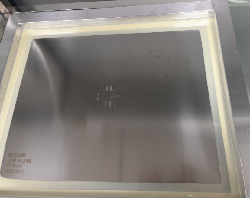
PCB stencils generally consist of a frame, wire mesh and steel plates. During the manufacturing process, the stencil is laser cut to ensure accuracy and consistency of the opening. This structural design allows the stencil to effectively meet the soldering needs of complex circuit boards while maintaining a high level of durability and stability.
PCB stencils generally consist of a frame, wire mesh and steel plates. During the manufacturing process, the stencil is laser cut to ensure accuracy and consistency of the opening. This structural design allows the stencil to effectively meet the soldering needs of complex circuit boards while maintaining a high level of durability and stability.
At present,there are four commonly used types of stencil in SMT processes based on manufacturing methods: mixed process stencil; Laser cutting of stencil; electroformed stencil and chemically etched stencil.
1.Chemical etching of stencil refers to the use of corrosive chemical solutions to remove the metal at the required hole position of stainless steel sheets, and obtain stencil corresponding to the PCB pad with the corresponding hole.
2.Laser cutting of stencil is a technology that uses high-energy laser beams to cut and drill holes on stainless steel sheets to obtain the required stencil. The laser cutting process of stencil is finely controlled by machines and is suitable for the production of ultra small spacing openings. Due to being directly ablated by laser, laser cutting of stencil holes has a straighter wall compared to chemical etching, without a conical shape in the middle, which helps to fill the mesh with solder paste.
3.Electroformed stencil is the most complex stencil manufacturing technology, which uses electroplating addition process to generate nickel sheets with the required thickness around the pre treated spindle. The biggest feature of electroformed stencil is its precise size, so there is no need for subsequent compensation treatment of hole size and hole wall surface.
4.Mixed process stencil is commonly referred to as the production process of stepped stencil. Stepped stencil retains two or more thicknesses on a stencil, which is different from a typical stencil with only one thickness. The main purpose of its production is to meet the different requirements of tin content for different components on the board.

In the PCB manufacturing process, the stencil is placed on the solder pads of the PCB board and a special scraper or brush is used to evenly apply solder paste to the stencil.
Solder paste is composed of solder powder and flux, which can adhere to the metal surface and form a good welding effect. By heating and pressure, the solder paste melts and reacts with the solder pads on the PCB board and the pins of electronic components, forming a good welding connection.
The role of stencil is mainly reflected in the following aspects:
1.Uniform application of solder paste:The stencil can ensure that the solder paste is evenly applied to the solder pads of the PCB board,avoiding omissions or excessive phenomena during manual application,thereby ensuring the quality and reliability of welding.
2.Positioning and fixation:The stencil can be accurately positioned and fixed on the solder pads of the PCB board,avoiding misalignment or detachment of components during the welding process,improving production efficiency and product quality.
3.Prevent bridging:The stencil can effectively prevent solder paste from bridging between solder pads, avoiding the occurrence of short circuits and improving the reliability and safety of the circuit.
4.Reduce defects:By using stencil,welding defects caused by uneven or omitted manual application, such as virtual welding and open circuits,can be reduced, improving the reliability and stability of the product.
5.Improve production efficiency:Using stencil can reduce manual operation time and cost,improve production efficiency, and automate production, further reducing production costs.
How to choose the right pcb stencil:
1.PCB size and specification
First of all,the size and specification of the PCB should be considered when choosing the right stencil. According to the desired PCB size, as well as aperture size, line width and line spacing and other factors, it is critical to choose the correct size of the stencil and aperture size. Ensure that the size of the PCB is smaller than the effective area of the stencil, so that the stencil can be effective solder paste printing.
2.Requirements of the mounter
When shopping for a stencil, it is critical to understand the requirements of the mounter. If the mounter has special size or specification requirements for the stencil, the designer should follow these requirements. By meeting the requirements of the mounter, unnecessary troubles and errors can be avoided in the production process.
3.Chip Pitch and Stencil Thickness
During the shopping process, it is also necessary to determine the minimum chip pitch on the target PCB board, which is crucial for selecting the thickness of the stencil. For large components, usually need a thicker PCB stencil to ensure good deposition of solder paste; while for small devices, usually use a thinner PCB stencil.
4.Aperture design
Proper aperture design is also important.The opening of the stencil should be designed according to the needs of different devices.For example,a stepped PCB stencil can be used to handle both large components and small components in order to thicken or thin according to the needs of each area.The natural trapezoidal design of the openings and control of dimensional errors should also be taken into account to ensure good solder paste release and print quality.
5.Materials and Coatings
Finally, considering the choice of stencil material, stainless steel is usually recommended.This is because stainless steel has good stiffness,corrosion resistance and ductility, which can directly affect the service life of the stencil. At the same time, choosing a stencil with the right coating can also help to improve quality and print accuracy.Ensure that the stencil you choose is able to withstand the environmental and operating conditions for each application.
The PCB stencil is a key process element in circuit board, which ensures that electronic components can be accurately and reliably soldered onto the PCB board,improving product quality and reliability.