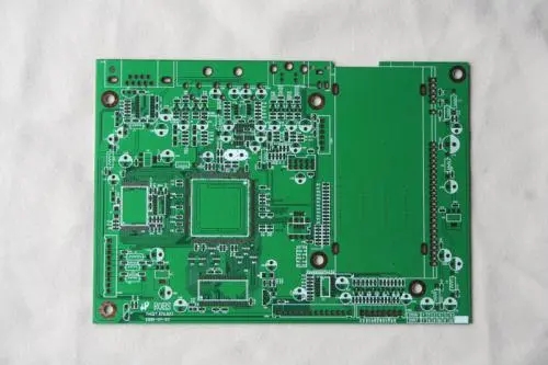
Whether the specifications and quality of the PCB board are good or not is related to the vital interests of our customers. How to test it? The following Shenzhen Loongson Century Reverse Technology Research Division will summarize the following common guidelines for you for your reference and modification .

1. Incoming goods should be consistent with the version of the purchase order;
2. There is no short circuit or open circuit in the line;
3. Non-line conductors (residual copper) must be more than 2.5mm away from the line, and the area must be ≤0.25mm2;
4. Holes are punched in the middle of the PAD, the hole position is offset or the PAD is damaged, and the single side is not less than 30%;
5. Over-drilling, leakage, deformation and end-penetration are not allowed in the drilling;
6. PTH parts plug-in hole, the broken hole area is less than 5%, and the paint (PAD on solder mask, the same below) area is less than 10%;
7. It is not allowed to warp the line (the line is warped);
8. The PAD of the PCB circuit must not be warped (the solder joint is warped);
9. It is not allowed to expose copper and tin in the circuit;
10. The actual line width shall not deviate from the original design width by ±20%;
11. The offset of the solder mask oil screen printing does not exceed ±0.15mm;
12. The line is painted, the painted area on the PAD must be ≤10% of the original area;
13. Blistering: the distance of the blistering area from the line must be ≤0.7mm or more, the maximum diameter ≤0.7mm2, and it is where the part is covered;
14. The shape tolerance is ±0.15;
15. The degree of PCB deformation, bending, and warping is ≤1% of the diagonal length of the substrate;
16. PCB is not allowed to be broken;
17. Orders signed to make goods shall be made on the basis of the last confirmed sample; goods signed for goods shall be made with the drawings of the signed drawing and its additional information;
18. If V-CUT is required for the jigsaw puzzle, the depth must be 1/3 of the thickness of the board;
19. Convex teeth or unevenness on the edge of the substrate ≤0.2mm;
20. The thickness of the gold plating must meet the requirements in APPROVE SHEET (single and double panels-5u);
21. The hole diameter is based on the molding dimension drawing provided in APPROVE SHEET, and the hole size and allowable error range are checked;
22. Because our factory has special requirements for white solder mask oil, if the PCB requires white oil, the white oil is pure white;
23. No fingerprints, water lines or wrinkles are allowed on the surface of the solder mask;
24. TEXT, MODEL, LOGO, FCC, CE and other text on the part surface must not be damaged or unrecognizable;
25. There should be no residue of flux, glue and other oil on the PCB surface;
26. If there are special requirements in the above terms, our company will notify you separately;
27. The final matters shall be resolved through consultation between the two parties.
The above is an overview of the PCB receiving standard. Ipcb is also provided to PCB manufacturers and PCB manufacturing technology.