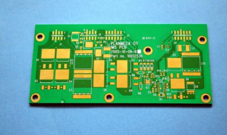
What is grounding ground?Whilst this question may seem simple,there are actually real differences between the different types of earthing. Electrical grounding refers to a conductor that acts as a common return path for current from various electrical devices,often referred to as the 0 potential point, the reference point for all other voltages in the system.
Chassis ground refers to the conductor that connects to the metal enclosure of the equipment,which is usually connected to the signal ground at one or more points. Determining where and how signal ground is connected to the chassis is critical to minimising noise and interference.Proper circuit grounding design reduces the radiated emissions of a product and increases its resistance to external electromagnetic fields.
In the case of a PCB, for example, when an input/output (I/O) cable is assembled in a metal enclosure, because the circuit ground carries current and has a certain impedance, it generates a voltage drop, VG. This voltage drives common mode currents on the cable, which in turn triggers radiation from the cable. If the circuit ground is connected to the chassis at the end of the PCB opposite the cable, the entire voltage VG drives current flow to the cable. However, if the circuit ground is connected to the chassis at the I/O connector, then ideally the voltage driving the common mode current flow to the cable will be zero. At this point, the entire ground voltage will be present at the end of the PCB where there is no cable connection. Therefore, it is critical to establish a low impedance connection between the chassis and circuit ground in the I/O area of the PCB.
Another explanation is that the ground voltage generates a common-mode noise current that flows to the I/O connector. At the connector, a shunt occurs between the cable and the point where PCB ground meets the chassis. the lower the value of the impedance from PCB ground to chassis, the lower the common-mode current on the cable. The key to achieving this approach is to be able to obtain a low impedance in the PCB to chassis connection (especially in the frequency range of interest). However, this is not usually easy to achieve, especially at frequencies in the range of several kilohertz or wider. At high frequencies, this means that low inductance is required, which usually needs to be achieved by multipoint connections.
Establishing a low impedance connection between circuit ground and chassis in the I/O area also helps improve radio frequency (RF) immunity. Any high-frequency noise currents induced into the cable will be conducted to the chassis instead of flowing through the PCB ground.
The chassis ground connection provides three major utilities:
As the chassis has been set to a global 0V reference potential, it now acts as a Faraday cage, providing extensive electromagnetic shielding.
It has a safety feature that effectively directs parasitic currents, including electrostatic discharges, short circuits or noise, back to earth.
At the input of the EMI filter, it provides a low impedance receive path for common mode noise, eliminating the need for additional ferrite or large chokes on the board.

About PCB grounding design:
01.Ground Layout
All components that need to be grounded are connected together by a common line, which is more common in older or simpler PCB designs.
02.Shared Ground Layer
The most common practice in PCB design is to set up a shared grounding layer, where any space on the PCB not occupied by an alignment or component is covered by the grounding layer.The shared ground plane not only significantly improves the thermal performance of the PCB, but also helps to reduce electromagnetic interference (EMI).
03.Dedicated Ground Layer Design
In multi-layer PCBs, a dedicated grounding layer is set up, and components are connected to the grounding layer through grounding vias.This design is more common in more layers and complex structure of the PCB.
04.Power system grounding configuration
During the installation of a power system,all grounding connections are summarised on a grounding bus.This bus is then connected to the grounding conductor and ultimately to the grounding rod or grounding network.
The grounding busbar concentrates the grounding conductors of all equipment to a common point.To ensure better grounding, the grounding resistance at this point should be less than 5 ohms, and a high gauge wire should be used to connect the grounding bus to the grounding devices (ground rods and grounding networks).
05.Equipotential earthing or uniform earthing
Equipotential grounding means that every conductive element within the protected area should have the same ground potential, which is achieved by electrically connecting the equipment chassis,metal pipework and all grounding devices.
Equipotential ensures that there is no significant difference in potential between any conductive components within the area, thus preventing electrocution in the event of a fault.
Earthing plays a vital role in electrical systems and equipment, not only providing a safe return path for equipment, but also reducing electromagnetic interference and improving system stability.Proper grounding design can effectively reduce common mode noise and radiation, thus improving the anti-interference capability and reliability of the equipment.We discuss chassis grounding and its application in PCB design,highlighting the importance of low-impedance connections and various grounding design strategies such as shared grounding layers and dedicated grounding layers.