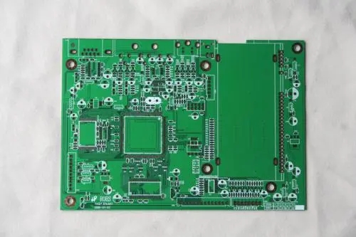
Before the layout design begins, a complete and detailed description of the circuit is required, mainly including the following aspects:
1) Schematic diagram, including details of components, connections, and edge connector specifications.
2) The component list, including the name, specification, model and manufacturer of the component.
3) Mechanical specifications, including the size and shape of the board, mounting holes, marking of the height-restricted area of components, and the location of edge connectors.
4) Printed circuit board specifications, single-sided, double-sided or multi-substrate, with or without plated through holes.
5) Pattern specifications, including the type and size of pads, the width and spacing of wires.
6) Electrical specifications, for example, the placement of components should be limited by the heat generated, capacitor or inductance donation, ground plane, critical length of wiring, etc.
7) Data manipulation.

First, prepare the component library, which describes the package type of each component required, including the shape, pad type, size, and pad location. In the complete component list, the package type of each component used, the name and location of the component, and the connection surface on the printed circuit board should be indicated. The connection form gives a precise description of all point-to-point connections. The final detailed information list of the circuit board contains board information and x/y coordinates at the corners of the board. The correctness of these form data, especially the connection form is extremely important. In many CAD systems, two independent operators are required to prepare connection sheets for the same circuit. Only after eliminating the differences between the two connection forms, is it possible to proceed to the next step.
A schematic diagram provides a graphical representation of the functional flow and circuit. The first step in the design of printed circuit boards using CAD systems is the input of schematic diagrams. A schematic system includes:
1) Electrical connection (network);
2) Connection point;
3) Integrated circuit symbol;
4) Symbols of discrete components, such as resistors, capacitors, transistors, etc.;
5) Input/output connector;
6) Power and ground symbols;
7) Bus;
8) Non-connected symbols;
9) Reference name of components;
10) Text description.
These symbols in the electrical schematic diagram should comply with international standards.
When the electrical schematic diagram is acquired, each graphic opened is a separate "project management window". If you need to process several graphics at the same time, you can open them all, each of which has its own "project management window". The "Project Management Window" is used to collect and organize all the resources needed by the project. These resources include schematic folders, schematic events, component libraries, components, and output reports, such as material lists and network tables. The management of a project does not actually include all the resources, but only points to the various files needed by the project. Therefore, never delete or move files related to any project. If deleted, these projects will no longer be able to find these files.
The above is an introduction to the steps of printed circuit layout design. Ipcb is also provided to PCB manufacturers and PCB manufacturing technology.