The overall process analysis of PCB design can be roughly divided into the following stages: netlist import, package library building, main design, physical and electrical constraint design, layout, wiring, design review, and design output. For a complex design, from the perspective of the task itself, layout and wiring are relatively the most onerous, especially wiring. From the long-term practical experience, manual wiring of important signals is still the main form of wiring.

Considering the complexity and arduousness of the placement and routing task process, a parallel design method is considered. Parallel PCB design methods for layout and routing are basically similar, but the objectives and focus are different. The following takes layout as an example, and a brief description will be made on the special points of parallel wiring design.
Task analysis and decomposition
The starting point of layout analysis is structural design constraints and circuit topology analysis. Structural design constraints include frame shape and size requirements, mounting holes and special component positioning and height limit requirements, and regional use constraints.

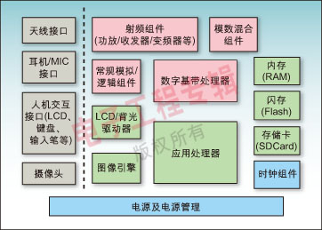
Consider a typical design example, taking mobile phone board design as an example. Observe from the circuit topology, the general principle block diagram is shown as in Fig. 1. Observing Figure 1 we can see that the signal characteristics of each part have obvious differences in the layout requirements. The layout of each component will be expanded according to the signal flow, and design requirements such as shielding and electromagnetic compatibility (EMC) should be taken into consideration. For product reliability and stability considerations, signal integrity (SI) issues must also be considered.
After analyzing the above-mentioned typical design examples, we can get a parallel design layout method: expand by circuit topology type, plan suitable space for each component, and arrange suitable engineers for parallel design layout.
Role arrangement
Taking Figure 1 as an example, consider the task decomposition of the following parallel design layout:
1. Communication protocol related groups, including radio frequency components (power amplifier/transceiver/inverter, etc.), analog-digital hybrid components, conventional analog/logic components, digital baseband processors, etc.;
2. Application related groups, including LCD/backlight driver, image processing engine, application processor, memory (RAM), flash memory (Flash), storage (SDCard), etc.;
3. Common signal related groups, including peripheral interfaces, power supply and power management, clock components, etc.
It is assumed that each of the parallel phases is assumed and completed by an engineer. Then there are the following role assignments: Engineer A is responsible for layout design and communication protocol group layout; Engineer B is responsible for application-related group layout; Engineer C is responsible for public signal-related group layout. The principle of role arrangement is to focus on the skills and expertise of each engineer.
Layout concurrent design

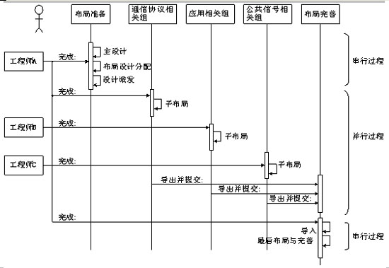
Figure 2 is a sequence diagram of parallel design. Among them: Engineer A prepares the main design (a staged design document that guides the entry of the netlist, performs structural constraint design, and locates the installation hole), plans the sub-layout material label according to the aforementioned decomposition method, and allocates the layout interval according to the design requirements, Make a task distribution description document; Engineer A divides the power generation principle design drawing, bill of materials, task distribution description document, PCB master design file, etc. to the other 2 engineers.
Each engineer (including Engineer A) carries out the layout according to their respective layout areas and related requirements. After the layout is completed, the devices that are not related to their tasks are deleted. Export the respective sub-layout files through the PCB tool software and submit them to the responsible engineer A.
After engineer A receives each sub-layout file, he still imports the sub-layout files to his own sub-layout file in turn through the PCB tool software. Engineer A makes the final layout adjustment and optimization according to the design requirements.
Parallel design of wiring
The starting point of wiring analysis is generally the analysis of the electrical signal of the circuit topology. Electrical signals can be divided into two types: critical signals (signals with strict electrical constraints) and non-critical signals.
Still considering the aforementioned mobile phone board design example, there are obvious differences in the wiring requirements of each part. The wiring of each component still needs to be expanded according to the layout elements and signal flow, while taking into account various electrical performance design requirements.
For the above-mentioned typical design examples, the following parallel design wiring method can be considered: the circuit topology type (that is, the required area division) and the signal flow are expanded to determine the wiring priority. For wiring with high priority (often with a large workload), wiring is given priority to ensure performance and progress.
Consider assigning parallel design tasks in the high-priority wiring tasks, and finally the responsible engineer will make the final improvement and finishing. In addition, the use of tools is different from the layout stage. The exported and imported files in the wiring stage will be sub-design files.
Summary of this article
After analyzing the principle of a mobile phone board design example, this paper describes the method of parallel design. Through the division of tasks and the combination of tools, the operation of parallel design is realized, which not only achieves the complementary advantages of resources, but also ensures the design quality and time schedule requirements.
The above is the introduction to parallel design of circuit boards.