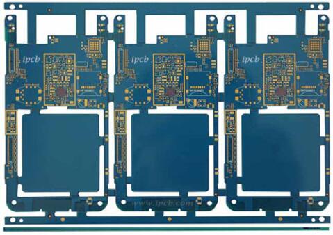
High-density interconnect (HDI) is one of the fastest-growing technologies in printed circuit board (PCB) design. Due to the more concentrated arrangement of smaller components, HDI board allow a higher circuit density than traditional circuit boards, thereby creating a more concise path. Blind vias and/or buried vias are commonly used to optimize the space on the HDI board, and now microvias with a diameter of 0.006 or less are often used.
Many vertical industries have integrated HDI boards into their products, including manufacturers of military communications and strategic equipment, and medical diagnostic tools. The lightweight design of the HDI board also makes it ideal for aerospace applications and smaller smartphones and laptops.

The most common types of HDI boards include:
1. Through holes from surface to surface
2. Combination of through holes and buried holes
3. Multiple HDI layers containing through holes
4. Passive mounting base plate for non-electric installation
5. Coreless construction by using layer pairs
6. Replace the coreless structure by using layer pairs
Benefits of HDI
For almost all applications related to aviation, consumer products, computers and electronic products, HDI boards are not only suitable but also popular. Even in a fierce environment, multilayer HDI boards can provide a higher level of reliability through the powerful interconnection of stacked vias.
The reduction in component size provides designers with more work space, thereby opening up both sides of the original PCB for design. Smaller components put together will generate additional input and output, thereby speeding up signal transmission, and greatly reducing cross delay and signal loss.
HDI technology can reduce the eight-layer through-hole PCB to a four-layer HDI micro-hole PCB, thereby reducing the number of layers that can achieve the same or better functions. This reduction greatly reduces material costs, making HDI technology very cost-effective for electronics manufacturers. The higher performance provided by the multi-layer HDI PCB makes it reliable even in harsh environments.
Why use HDI?
Due to its light weight, reliable performance and small size, HDI boards are particularly suitable for wearable, mobile and handheld electronic devices. These stronger, smaller components and more transistors combined with high-density design geometries enhance the functionality of PCBs and their final products.
Components are closer to each other, so it takes less time for electrical signals to propagate. The high-density design of the HDI board reduces the rise time of the signal and inductance, thereby limiting the impact on nearby pins and leads. The additional transistors not only support the added functionality, but also improve performance.
Focusing on HDI design can reduce the time and cost of training prototypes, shorten delivery time, and obtain greater profit margins.
HDI technology can produce products that are lighter, faster and more efficient, and use smaller packaging. The reduction in size makes it possible to design smaller end products that can meet consumer demand for portability. For designers, HDI can be a time-consuming training job. However, as market relevance increases, the rewards of productivity, reliability, and fewer manufacturing delays make the training time worthwhile.