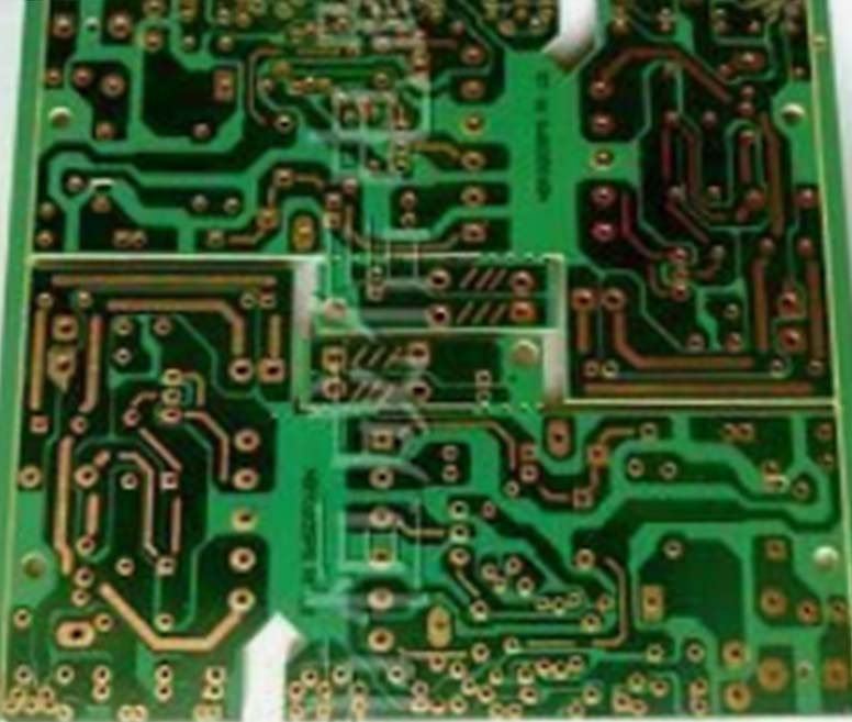
PCB smart home board is the key hardware carrier for realising smart home functions.It integrates a variety of electronic components,such as microprocessors, sensors, communication modules, etc., and connects these components through precise circuit design to form an efficient and synergistic working system.
For example,it senses the indoor temperature through temperature sensors,and then the microprocessor controls the operation of the air conditioner according to the preset temperature range to achieve intelligent temperature regulation.At the same time, it is also responsible for data transmission and processing to ensure interconnectivity between smart devices.Whether it is the control of smart lights, the security of smart door locks, or the remote operation of smart home appliances, the PCB smart home board is indispensable for its precise operation.
PCB smart home board features
1.Miniaturisation: small size, easy to install in various smart home devices.
2.High integration: contains a variety of functional modules, such as processors, communication modules, sensor interfaces and so on.
3.Low power consumption: to meet the needs of smart home devices running for a long time.
4.High stability: to ensure reliable operation of the system.

Key factors to consider when designing a PCB smart home board:
1.Device analysis and requirements
Understanding the purpose and function of smart home devices is the first step in design.This involves a thorough requirements analysis to identify the required sensors, electronics, actuators, communication modules and power management components.This step is critical for subsequent design.
2.Prototyping and Conceptualisation
During the design process, the functions and features of the smart home device need to be conceptualised.Prototyping involves creating pre-structures to validate and test the idea of the device in order to select the right components that match the functionality and reliability.
3.Circuit Schematic Design
This step includes drawing circuit schematics that depict the electrical connections and structure of the components on the PCB board.This process helps to visualise the actual design or layout diagram.
4.PCB Layout Design
After completing the circuit schematic, the next step is to design the actual layout of the PCB.This process requires the use of specific software (e.g.Altium, KiCAD, Eagle, etc.) to assemble, integrate and connect the components to the PCB board.
5.Power Management
Smart home devices require efficient power management solutions to optimise energy consumption and ensure reliable operation.This can be achieved by integrating voltage regulators, switching power supplies and battery charging circuits to ensure efficient power supply within the smart home system.
6.Wireless Connectivity
Considering that most smart home devices rely on wireless communication, careful consideration must be given to the layout of the wireless modules to ensure effective antenna placement and signal integrity to avoid interference.
7.Signal Integrity
When designing a PCB, it is critical to ensure signal integrity under all operating conditions.This can be achieved through appropriate impedance matching techniques, reducing the length of signal alignments and using power planes.
8.Security and Privacy
Security and privacy must be considered during design.Smart home PCBs should have measures to protect user data and communication security, such as integrated encryption modules, secure authentication chips and tamper-proof circuits.
9.Size and space constraints
Smart home devices usually require miniaturisation, so the design must pay attention to the size and layout of components to ensure reasonable placement and functionality within the limited PCB space.
10.Thermal Management
Considering that high power components generate heat, heat must be effectively managed in PCB design to prevent overheating leading to component failure.This can be achieved through hot pads, heat pipes, or by incorporating an appropriate cooling system into the design.
As the smart home market continues to expand and technology continues to innovate, the demand for PCB smart home boards will continue to grow.Jettop will continue to increase its investment in R&D and production to continuously improve its technology and product quality.On the one hand, we will strengthen cooperation with chip manufacturers, smart device manufacturers and other enterprises upstream and downstream of the industry chain to jointly promote the development of smart home technology; on the other hand, we will continue to pay attention to the changes in market demand, and optimise our customised services to provide our customers with higher quality and more efficient solutions.We believe that in the future, JDobang will make more brilliant achievements in the field of PCB smart home boards,bring more convenience and surprises to people's smart life, and help the smart home industry move towards a better future.
In conclusion, PCB smart home board, as the core hardware of smart home system, has powerful functions and broad application prospects.With the continuous progress and innovation of technology, PCB smart home board will continue to develop and improve, bringing more convenience and surprise for people's smart life.