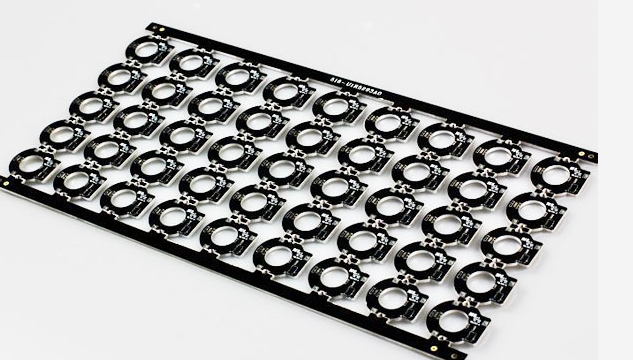
The design and production of circuit boards have certain processes and precautions. The copper coating of circuit boards is a crucial step in PCB design and has a certain technical content. So how to do the design work of this link, there are senior engineers Summarized a few experiences:
Everyone knows that under high frequency conditions, the distributed capacitance of the wiring on the printed circuit board will work. When the length is greater than 1/20 of the corresponding wavelength of the noise frequency, an antenna effect will occur, and the noise will be emitted through the wiring. If there is a poorly grounded copper pour in the PCB, the copper pour becomes a tool for spreading noise. Therefore, in a high-frequency circuit, do not think that the ground wire is connected to the ground. This is the "ground wire". ", be sure to punch holes in the wiring with a spacing less than λ/20, and "good ground" with the ground plane of the multilayer board. If the copper coating is handled properly, the copper coating not only increases the current, but also plays a dual role of shielding interference.
In copper coating, in order to achieve the desired effect of copper coating, those issues need to be paid attention to in copper coating:

1. If the PCB has many grounds, such as SGND, AGND, GND, etc., according to the position of the PCB board, the main "ground" is used as a reference to independently pour copper, digital ground and analog ground. It is not necessary to separate the copper pour. At the same time, before the copper pour, first thicken the corresponding power connection: 5.0V, 3.3V, etc., in this way, multiple deformed structures with different shapes are formed.
2. For single-point connections to different grounds, the method is to connect through 0 ohm resistors or magnetic beads or inductance.
3. The copper pour near the crystal oscillator, the crystal oscillator in the circuit is a high-frequency emission source, the method is to pour copper around the crystal oscillator, and then ground the shell of the crystal oscillator separately.
4. The island (dead zone) problem, if you think it is too big, it won't cost much to define a ground via and add it in.
5. At the beginning of PCB wiring, the ground wire should be treated the same. When routing the ground wire, the ground wire should be routed well. You cannot rely on adding vias to eliminate the ground pins for the connection after copper plating. This effect is very bad. .
6. It is best not to have sharp corners on the board (<=180 degrees), because from the perspective of electromagnetics, this constitutes a transmitting antenna! There will always be an impact on others, but it is big or small That's it, I recommend using the edge of the arc.
7. Do not pour copper in the open area of the middle layer of the multilayer board. Because it is difficult for you to make this copper clad "good ground".
8. The metal inside the device, such as metal radiators, metal reinforcement strips, etc., must be "good grounding".
9. The heat dissipation metal block of the three-terminal regulator must be well grounded. The ground isolation strip near the crystal oscillator must be well grounded. In short: if the grounding problem of the copper on the PCB board is dealt with, it is definitely "pros outweigh the disadvantages". It can reduce the return area of the signal line and reduce the electromagnetic interference of the signal to the outside.