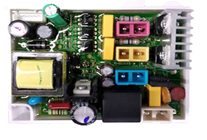
The PCB layout forms the basis of a well-functioning and robust PCB. Ignoring various PCB layout guidelines can lead to increased costs, poor PCB performance, and even circuit board failure.
There are many layout tips and guidelines available; however, it lists layout techniques that are believed to be applicable to many PCB designs.
1. Leave enough space between the traces. If the traces are accidentally connected during the PCB manufacturing process, placing the pads and traces too close will increase the risk of short circuits. We recommend leaving a gap of 0.007" to 0.010" between all adjacent pads and traces on the circuit board.
2. Balance the copper on each side of the PCB by using ground fillers on the other side of the dense copper pattern side.
3. Reduce EMI by implementing closely spaced, adjacent solid planar return paths for signal traces.

4. Avoid using a 90-degree trace angle. During the PCB manufacturing process, the outer corners of the 90-degree trace may be etched to be narrower than the standard trace width. Therefore, try to use a 45-degree trajectory.
5. Widen the power and ground traces. Wider power and ground traces allow more current to flow through them and reduce heat build-up, which can damage your circuit boards and wires.
6. Use vias to dissipate heat. Vias provide electrical connections between layers. But the heat dissipation hole can be used as a way to transfer heat from the heat generating component to the area where it can be dissipated.
7. Use a solid copper layer to form the power layer for EMI shielding and heat dissipation.
8. Add the reference point to the same side of the PCB where the SMT part will be placed. Surface mount assembly machines use fiducial marks to ensure the correct orientation of the PCB, which is necessary for component placement.
9. Use power layers to distribute power to almost all areas of the PCB. Power planes can be created by adding copper layers to the stack and connecting them to power or ground.
0. Consider using buried vias in very dense designs to allow the area above and below the buried vias to be used for additional wiring.
11. Use a unique drill size symbol for each type of hole that contains the same attributes. For example, if there are several 0.028-diameter holes on a PCB with the same plating requirements and hole diameter tolerances,
Then they can all be assigned the same symbol. However, if there are some 0.028 diameter holes with different characteristics, such as different drilling tolerances or plating requirements, different drilling symbols should be used on the drawing.
12. Create a symmetrical stack by alternating the signal and plane layers symmetrically around the centerline of the PCB.
13. Choose a trace width that your PCB manufacturer can easily manufacture.
14. Route all critical signals to establish the shortest path and as few vias as possible, while keeping the return path adjacent to the solid plane.
15. To facilitate circuit board testing, many test points are connected to the power and ground network. These test points can be accessed across the PCB.
16. Avoid placing test points near or near tall components, as this will make it difficult to evaluate test points.
17. Leave space between the trace and the mounting hole. Consider leaving enough space around the mounting holes to avoid contact with surrounding components and traces, otherwise it may cause an electric shock hazard on your circuit board.
18. Reducing the trace width requires proportionally reducing the height (or thickness) of the trace, and PCB stacking needs to show this detail.
Failure to reduce the thickness of the copper may cause the copper at the bottom to be too narrow and fail. The reason is that in the PCB printing and etching process, the traces in contact with the substrate material are more susceptible to acid erosion, resulting in a trapezoidal effect.