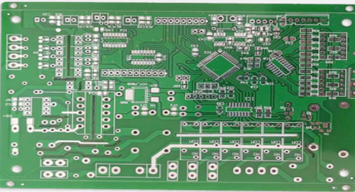
The power bus is one of the problems of EMI. There are many ways to solve the EMI problem. Modern EMI suppression methods include: using EMI suppression coatings, selecting appropriate EMI suppression parts, and EMI simulation design. This article discusses the problem of power bus in multi-layer PCB
Power bus
Properly placing a capacitor of appropriate capacity near the power supply pin of the IC can make the IC output voltage jump faster. However, the problem does not end here. Due to the limited frequency response of capacitors, this makes the capacitors unable to generate the harmonic power required to drive the IC output cleanly in the full frequency band. In addition, the transient voltage formed on the power bus bar will form a voltage drop across the inductor of the decoupling path. These transient voltages are the main common mode EMI interference sources. How should we solve these problems?
As far as the IC on our circuit board is concerned, the power layer around the IC can be regarded as an excellent high-frequency capacitor, which can collect the part of the energy leaked by the discrete capacitor that provides high-frequency energy for clean output. In addition, the inductance of a good power layer should be small, so the transient signal synthesized by the inductance is also small, thereby reducing common mode EMI.

Of course, the connection between the power layer and the IC power pin must be as short as possible, because the rising edge of the digital signal is getting faster and faster, and it is best to connect it directly to the PCB pad where the IC power pin is located. This needs to be discussed separately.
In order to control common-mode EMI, the power plane must help decoupling and have a sufficiently low inductance. This power plane must be a well-designed pair of power planes. Someone may ask, how good is good? The answer to the question depends on the layering of the power supply, the material between the layers, and the operating frequency (that is, a function of the IC rise time). Generally, the spacing of the power layer is 6mil, and the interlayer is FR4 material, the equivalent capacitance of the power layer per square inch is about 75pF. Obviously, the smaller the layer spacing, the greater the capacitance.
There are not many devices with a rise time of 100 to 300 ps, but according to the current IC development speed, devices with a rise time in the range of 100 to 300 ps will occupy a high proportion. For circuits with a rise time of 100 to 300ps, 3mil layer spacing will no longer be suitable for most applications. At that time, it was necessary to use layering technology with a layer spacing of less than 1 mil, and to replace FR4 dielectric materials with materials with high dielectric constants. Now, ceramics and ceramic plastics can meet the design requirements of 100 to 300 ps rise time circuits.
Although new materials and new methods may be used in the future, for today's common 1 to 3ns rise time circuits, 3 to 6mil layer spacing and FR4 dielectric materials, it is usually sufficient to handle high-end harmonics and make the transient signal low enough, that is to say, Common mode EMI can be reduced very low. The PCB layered stacking design examples given in this article will assume a layer spacing of 3 to 6 mils.