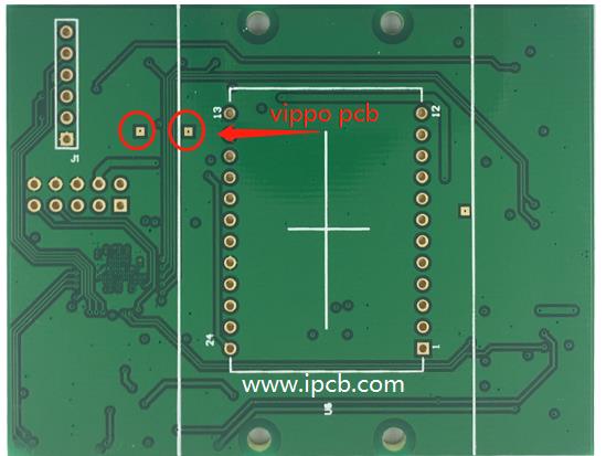
VIPPO (Via in Pad Plated Over), which stands for (Via on Pad) or (Plated Over Vias) marking, is a specialised technique used in printed circuit board design that involves the placement of via holes directly on the surface mount pads of components. It is a very useful technique that is actually suitable for high density PCB designs where space is the main constraint and routing of alignments is becoming more and more challenging, that's why we use these techniques to optimise our PCB designs within the given available space, this technique also reduces the size of the PCB and improves signal integrity.
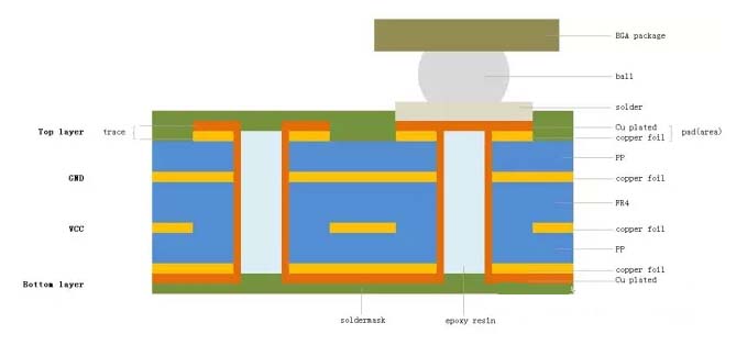
VIPPO technology involves two major steps in the manufacturing process: drilling and plugging. Unlike traditional full or half plugs,VIPPO adds a Cu cap flush with the pad at the top of the via after plugging, which solves the problem of solderability and prevents solder paste or flux from flowing into the hole during SMT to avoid the generation of gases that can affect the quality of soldering.The production process of VIPPO is shown in the figure below. Unlike a normal via, it wears a Cu cap, which is flush with the pad.

vippo
The most difficult thing to control with vippo PCB plug holes is the solder balls or ink pads in the holes, also known as oil popping. Some ipcb customers have very strict requirements on soldermask and appearance. Among them, PCB production has requirements for vippo plugging holes,and the most difficult thing to control when we used to produce PCBs is the problem of oil burst after curing or tin spraying, which leads to soldermask on the pads and the problem of solder balls in the holes. Curing or tin spraying is the process of hole plugging ink solvent volatilisation and resin shrinkage. Therefore, improper control is most likely to cause tin beads or oil explosion in the hole.
The via hole is drilled directly on the solder joint. In order to ensure that the soldering performance of the solder joint is not affected, resin is usually used to plug the hole, and then the surface of the via hole is plated so that the hole cannot be seen on the surface, so it is called For vippo. Vippo plays two roles: first, it plays a role in the conduction between the layers; second, after plugging the hole, the surface of the hole is plated, so that it will not affect the welding performance of the solder joint.
The inner diameter of the pad of the vippo PCB,after passing through the resin plug hole, a layer of copper is deposited on the inner diameter substrate to make the surface look like a large copper surface, and the hole is buried under the pad. Vippo PCB can increase the surface pad area.For small line width and line spacing, PCB wiring, when the pad area is small, it can reduce the area and reduce the size of the PCB while completing the continuity.
Our common vippo is mainly used in the packaging area of BGA, because when its surface needs to be soldered or chip attached, its accuracy and acceptable area are high, and the flatness of the surface is also high, preventing the unevenness of the chip from causing false Welding or joints are poor, so we recommend the regular surface treatment to be chemical nickel gold.
The customer requires that the hole needs to be plugged with a certain material (conventional 0.6mm or less), and when electroplating is filled, the vippo process is used. In the BGA area, the vias are punched on the BGA solder joints, combined with the patch layer, the soldering layer, and the solder mask layer to determine whether it is a vippo PCB. The size of the vias in the BGA area is generally below 0.3mm, and the solder joints are generally 10mil. Left and right, judge whether it is a vippo PCB by the size of D code.

vippo PCB
The signal integrity enhancement achieved by VIPPO (Via-in-Pad Plated Over) technology is mainly due to its unique design and manufacturing methodology.
1.Reduced fan-out length
VIPPO technology allows via holes to be placed directly below the pads of surface mounted devices (SMDs).This design allows for a significantly shorter fan-out path for signals travelling from the component to other layers of the PCB, thus reducing the distance required for signal propagation.The short fan-out length not only reduces inductance and resistance, but also reduces signal reflection and distortion, improving the quality of signal transmission.
2.Reduction of parasitic inductance
With VIPPO technology, the impact of parasitic inductance is reduced due to the optimisation of the signal line design.Whereas conventional through-hole designs result in additional inductance between component pads and other circuitry, VIPPO reduces signal losses by avoiding additional connection paths.This is especially important for high frequency signals, which are more susceptible to parasitic inductance during transmission.
3.Improved Electrical Connections
VIPPO technology fills the via hole and then copper plates the top to form a flat electrical connection, which not only improves mechanical strength, but also improves solderability and avoids connection problems caused by solder flowing into the via hole.A reliable electrical connection is critical to signal integrity as it ensures stable signal transmission.
4.Optimising the signal transmission path
In designs using VIPPO, the current path is more straight-through due to the direct connection between the through-hole and the component, which reduces impedance mismatches that can occur in signal transmission.By optimising the signal transmission path, signal reflection and attenuation can be effectively reduced, thus maintaining signal integrity.
5.Reduce Thermal Problems
VIPPO technology enhances the heat dissipation capability of the board by improving the filling structure of the vias.This improved thermal performance helps maintain the operating temperature of the entire board, further enhancing signal integrity, especially in high power and high frequency applications.
6.High Speed Signal Support
VIPPO technology is particularly suitable for high-speed interfaces (e.g.USB-C, HDMI, etc.), and its application in the BGA area reduces signal loss and crosstalk in high-frequency situations.This makes VIPPO in the strict requirements of high-speed electronic equipment, can effectively improve signal stability and transmission speed.
VIPPO technology significantly improves PCB signal integrity through sound design concepts, efficient manufacturing processes and optimised electrical connections, ensuring signal quality in modern high-density and high-frequency board designs.