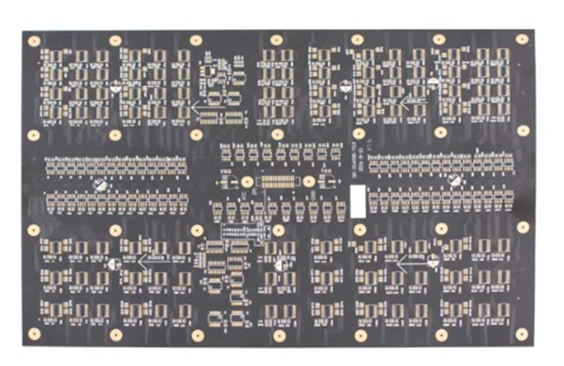
In the industry, a printed circuit board (PCB) with a copper foil thickness equal to or greater than 105 μm (≥3 oz) is called a thick copper printed circuit board.The application field and demand for thick copper PCB have been rapidly expanded in recent years, and it has become a popular PCB variety with good market development prospects.
Compared to conventional PCBs,thick copper PCB has a significant increase in copper foil thickness. Conventional PCBs usually have a copper foil thickness of tens to hundreds of microns, such as 18μm, 35μm, etc.Thick copper PCBs are much thicker. Thick Copper PCBs have much thicker copper foils, commonly 3oz, 4oz or even higher.
This increase in thickness makes the performance of thick copper PCBs very different from that of conventional PCBs. Firstly, thick copper PCBs are more conductive and can carry higher currents, making them suitable for high power electronic devices. Secondly, thick copper PCBs also have better heat dissipation properties, which can effectively dissipate the heat generated during the working process and ensure the stable operation of electronic devices.
The vast majority of thick copper printed circuit boards are high-current substrates, and high-current substrates are mainly used in two areas: power modules (power modules) and automotive electronic components. The development trend of this kind of high-current substrate is to carry a larger current, and the heat from a larger device needs to be dissipated, and the thickness of the copper foil used for the substrate is getting thicker.For example, the use of 210 μm thick copper foil for high-current substrates has become commonplace; another example is to replace the original busbars and wiring harnesses used in automobiles,robots,and power supplies.The thickness of the conductor layer of the substrate has reached 400 μm. ~2000 μm.

Inkjet printing process technology for thick copper plates
For power supply boards and coil boards with high current-carrying capacity and high voltage resistance requirements, thick copper with a copper thickness of more than 5oz, due to the high copper surface of the line, the traditional dry film and wet film screen-printed soldermask inks need to be screen-printed and exposed and developed for 2-3 times to achieve a specific ink thickness, which is a relatively long process. For 5OZ and thicker copper boards, the use of printing and caulking + screen printing surface oil can save production processes, improve efficiency, and at the same time can quickly achieve productisation.

Traditional thick copper pcb solder resist printing process is:
Soldermask pre-treatment → soldermask printing (using plus 80-150ml open oil and water ink) → static 2-3H → pre-bake → test → exposure → development → test → soldermask curing → soldermask pre-treatment (not open grinding brush) → printing (using plus 80-130ml open oil and water ink) → static 2H → pre-bake → test → exposure → development → test → post-curing
Disadvantages of the traditional process:
① ink wrinkles:due to the thick copper plate copper and the substrate of the fall is too large, solder resist printing copper surface and the substrate position of the ink will be thicker, the ink is too thick will cause ink wrinkles.
② ink bubbles:ink is too thick when the ink bubbles within the ink is more difficult to discharge discharge, pre-bake caused by ink bubbles.
③ Process time is long:static time is too long, static process is easy to ink moisture absorption caused by the reliability of unqualified.
After using the above process,the bottleneck of the smooth mass production of copper printed circuit boards with a thickness of 105 mm or more has been solved, and the scrap rate has been reduced from 1.2% to 0.3%, making the copper printed circuit boards with a thickness of 105 mm or more used in power products, And the fields of communication, electric power, and aerospace have been guaranteed.