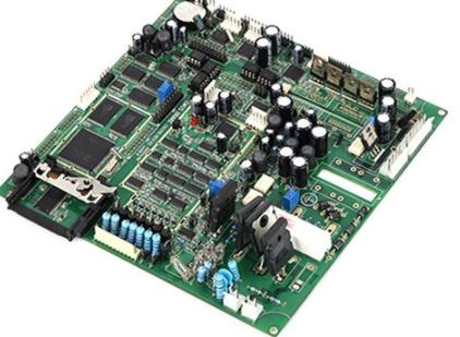
PCB layout is a process before PCB processing. How to design so that the files you draw can effectively meet the production requirements of PCB processing factories?
1. Welding ring (Ring ring): The welding ring of the PTH (copper-plated hole) hole must be 8mil larger than the one side of the drilled hole, that is, the diameter must be 16mil larger than the drilled hole. The welding ring of the Via hole must be 8mil larger than the one side of the drilled hole, and the diameter must be 16mil larger than the drilled hole. In short, whether it is through-hole PAD or Via, the inner diameter must be greater than 12mil, and the outer diameter must be greater than 28mil. This is very important!
2. The line width and line spacing must be greater than or equal to 4 mils, and the distance between holes should not be less than 8 mils.
3. The etching word line width of the outer layer is greater than or equal to 10 mils. Note that it is etching and not silk screen.
4. The circuit layer is designed with a grid board (copper is paved into a grid), the rectangle of the grid space is greater than or equal to 10*10mil, that is, the line spacing should not be less than 10mil when the copper is laid, and the grid line width is greater than or equal to 8mil.
When laying a large area of copper skin, it is recommended to set it into a mesh for the materials.

First, it can prevent the substrate of the PCB board and the adhesive of the copper foil from generating volatile gas when dipping or heating, and the heat is not easy to be removed, causing the copper foil to expand and fall off;
Secondly, the more important thing is that the thermal performance and high-frequency conductivity of the grid-like floor are much better than the solid floor of the whole piece. But I think that in terms of heat dissipation, the advantages of copper grids cannot be generalized.
It should be considered that in the case of local heating that will cause PCB deformation, grid copper should be used to lose heat and maintain the integrity of the PCB. The advantage of this kind of copper is that the temperature of the board surface is certain. Improved, but still within the scope of commercial or industrial standards, the damage to components is limited; but if the direct consequence of PCB bending is the appearance of virtual solder joints, it may directly lead to line failure.
The result of the comparison is to use less damage as the best. The real heat dissipation effect should be solid copper. In practical applications, the copper in the middle layer is basically seldom grid-like, that is, the uneven stress caused by temperature is not as obvious as the surface layer, and solid copper with better heat dissipation effect is basically used.
5. The distance between the NPTH hole and the copper is greater than or equal to 20 mils.
6. For the board formed by the gong board (milling cutter), the distance between the copper and the forming line is greater than or equal to 16 mils; therefore, the distance between the trace and the frame should not be less than 16 mils during layout. In the same way, when slotting, the distance to copper must be greater than or equal to 16 mils.
7. For die-punched boards, the distance between the copper and the molding line is greater than or equal to 20 mils; if the board you draw may be mass-produced in the future, in order to save costs, mold opening may be required, so it must be foreseen when designing .
8. V-CUT (usually draw a line on the Bottom Mask and Top Mask layers, it is best to mark the place where V-CUT is required) The formed board should be designed according to the thickness of the board;
1. The board thickness is 1.6mm, and the distance between the copper and the V-CUT line is greater than or equal to 0.8mm (32mil).
2. The board thickness is 1.2mm, and the distance between the copper and the V-CUT line is greater than or equal to 0.7mm (28mil).
3. The thickness of the board is 0.8mm-1.0mm, and the distance between the copper and the V-CUT line is greater than or equal to 0.6mm (24mil).
4. The board thickness is less than 0.8mm, and the distance between the copper and the V-CUT line is greater than or equal to 0.5mm (mil).
5. For the golden hand board, the distance between the copper and the V-CUT line is greater than or equal to 1.2mm (mil).
Note: Don't set such a small spacing when jigsaw puzzles, try to be as large as possible.
The above is an introduction to the design rules of the outer circuit of the PCB layout