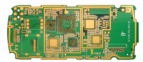
One of the most important aspects of electronic product design is PCB layout. Therefore, Advanced Circuits provides PCB Artist, a free professional PCB layout software that allows you to create up to 28 layers of PCBs and easily integrate them into your PCBs using its library of more than 500,000 components. When you use PCB Artist to create a printed circuit board layout, you can place your manufacturing order directly through the software, making it easier to transfer the layout file to us for manufacturing, because you know your design will be produced as expected. If you are designing a printed circuit board for the first time, here are some general tips to help you achieve a perfect layout.
Check the manufacturer's tolerances & features before starting to use the PCB layout

Before starting, it is best to check the functions and manufacturing specifications of the PCB manufacturer in order to set up the PCB layout software accordingly. If you have completed the PCB layout and want to check whether it meets all manufacturing requirements, you can use our FreeDFM tool to upload your Gerber file and run a manufacturability check within a few minutes. You will receive a detailed report on any manufacturability issues found in the PCB layout sent directly to the inbox. Every time you run the PCB layout through the FreeDFM tool, you can also get a discount code to use advanced circuits in PCB manufacturing orders, up to $100.
Determine the number of layers required for PCB layout
It is important to determine the number of layers required for the PCB layout that best suits your application and functional requirements. Although more layers can help accommodate more complex designs and functions and take up less space, keep in mind that more conductive layers will also increase production costs.
Consider the space requirements of PCB layout
Calculating the physical space that the printed circuit board layout can take up is the key. Depending on the final application and requirements, space may also be a limitation and cost driver. Consider not only the space required for components and their tracks, but also circuit board mounting requirements, buttons, wires and other components or other circuit boards that are not part of the PCB layout. Estimating the size of the circuit board from the beginning can also help you calculate production costs.
Determine any specific component placement requirements
One of the key steps in the circuit board layout process is knowing how and where to place components, especially when the location of a particular component is forced by factors other than the function of the circuit board itself; such as buttons or connection ports. At the beginning of the board layout process, you should develop a rough plan detailing where to place the main components so that the most convenient design can be evaluated and used. Try to leave a distance of at least 100 mils between the component and the edge of the printed circuit board, and then place the component that requires a specific location first.