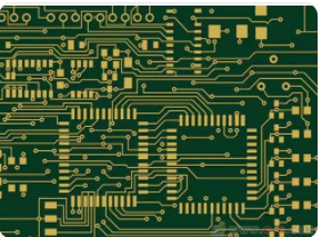
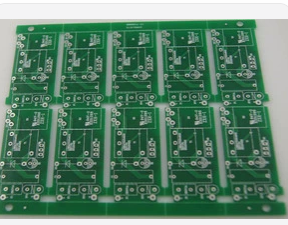
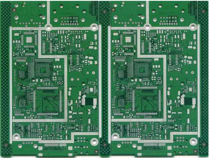
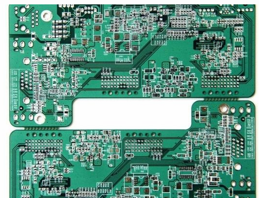
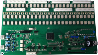
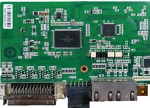
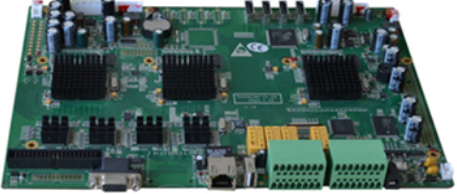
Copy PCB board, the industry is often called circuit board copy board, circuit board clone, circuit board copy. copy PCB board is a kind of reverse research technology, which is to obtain the PCB design circuit of an excellent electronic product through a series of reverse research technology, as well as circuit schematic diagram and BOM table.
Misunderstanding
The process of copy PCBing can realize the rapid update, upgrade and secondary development of various types of electronic products through the extraction and partial modification of technical data files. Willing to optimize the design and board modification of the PCB, and can also add new functions to the product or redesign the functional features on this basis, so that products with new functions will be unveiled at the fastest speed and with a new attitude. With its own intellectual property rights, it has also won the first opportunity in the market, bringing double benefits to customers.
Technical process
The technical realization process of copy PCB board
To put it simply, first scan the circuit board to be copied, record the detailed component location, and then remove the components to make a bill of materials (BOM) and arrange the material purchase, and the empty board is scanned into a picture and copied by the board software The processing is restored to a PCB board drawing file, and then the PCB file is sent to the plate making factory to make the board. After the board is made, the purchased components are soldered to the made PCB board, and then the circuit board is tested and debugged.

The specific technical steps are as follows:
The first step is to get a PCB. First, record the model, parameters, and positions of all components on the paper, especially the direction of the diode, the transistor, and the direction of the IC gap. It is best to use a digital camera to take two photos of the location of the components. Many PCB circuit boards are becoming more and more advanced. Some of the diode transistors on the above are not noticed at all.
The second step is to remove all the components and remove the tin in the PAD hole. Clean the PCB with alcohol and put it into the scanner. When the scanner scans, you need to raise the scanned pixels slightly to get a clearer image. Then lightly polish the top and bottom layers with water gauze until the copper film is shiny, put them in the scanner, start PHOTOSHOP, and scan the two layers in separately in color. Note that the PCB must be placed horizontally and vertically in the scanner, otherwise the scanned image cannot be used.
The third step is to adjust the contrast, brightness and darkness of the canvas to make the part with copper film and the part without copper film have a strong contrast, then turn the second image into black and white, and check whether the lines are clear. If not, repeat this step. If it is clear, save the picture as black and white BMP format files TOP BMP and BOT BMP. If you find any problems with the graphics, you can also use PHOTOSHOP to repair and correct them.
The fourth step is to convert the two BMP format files to PROTEL format files, and transfer two layers in PROTEL. For example, the positions of PAD and VIA that have passed through the two layers basically coincide, indicating that the previous steps are well done. If If there is a deviation, repeat the third step. Therefore, copy PCBing is a work that requires patience, because a small problem will affect the quality and the degree of matching after copying.
The fifth step is to convert the BMP of the TOP layer to TOP PCB. Pay attention to the conversion to the SILK layer, which is the yellow layer. Then you can trace the line on the TOP layer and place the device according to the drawing in the second step. Delete the SILK layer after drawing. Repeat until all the layers are drawn.
The sixth step is to import TOP PCB and BOT PCB in PROTEL and combine them into one picture and it will be OK.
The seventh step, use a laser printer to print TOP LAYER and BOTTOM LAYER on transparent film (1:1 ratio), put the film on that PCB, and compare whether there are errors. If they are correct, you are done.
Double-sided copy board method:
1. Scan the upper and lower layers of the circuit board and save two BMP pictures.
2. Open the copy board software Quickpcb2005, click "File" "Open Base Map" to open a scanned picture. Use PAGEUP to zoom in on the screen, see the pad, press PP to place a pad, see the line and follow the PT line...just like a child drawing, draw it in this software, click "save" to generate a B2P file.
3. Click "File" and "Open Base Image" to open another layer of scanned color image;
4. Click "File" and "Open" again and open the B2P file saved earlier. We see the newly copied board, stacked on top of this picture-the same PCB board, the holes are in the same position, but the circuit connections are different . So we press "Options"-"Layer Settings", turn off the top-level circuit and silk screen here, leaving only multi-layer vias.
5. The vias on the top layer are in the same position as the vias on the bottom picture. Just trace the lines on the bottom layer just like in childhood. Click "Save" again-the B2P file now has two layers of information on the top and bottom layers.
6. Click "File" and "Export as PCB File", and you can get a PCB file with two layers of data. You can change the board or output the schematic diagram or send it directly to the PCB plate factory for production.
Multilayer board copy method:
In fact, the four-layer board copying board is repeated copying two double-sided boards, and the sixth layer is repeated copying three double-sided boards... The reason why the multi-layer board is daunting is because we can't see the internal wiring. How do we see the inner layers of a precision multilayer board? -Stratification.
There are many ways to deal with the problem of layering, such as corrosion of potions and stripping of tools, but it is easy to over-separate layers and lose data. Experience tells us that sandpaper polishing is the most accurate.
When we finish copying the top and bottom layers of the PCB, we usually use sandpaper to polish the surface layer to show the inner layer; sandpaper is ordinary sandpaper sold in hardware stores, generally flat PCB, and then hold the sandpaper and rub evenly on the PCB (If the board is small, you can also flatten the sandpaper, and rub the sandpaper while pressing the PCB with one finger). The main point is to pave it flat so that it can be ground evenly.
Reliability design of copy PCB board contact system
The correct choice of contact material can improve the reliability and life of the relay IRF520NPBF. Different relays have different types and degrees of wear on the contacts due to the different load properties and disconnecting capacities of the contact circuits; these factors must be considered when designing and selecting contacts and reed materials. The selected contact and reed materials should meet the following basic requirements:
1. It has good electrical conductivity and thermal conductivity.
2. The contact and coating materials should be able to withstand arc or electric spark abrasion and mechanical abrasion, and have certain hardness and anti-adhesion properties.
3. The reed material should have good elasticity.
2) Requirements for contact contact form and shape and size design:
1. For the relays with small load such as miniature and subminiature, the contact should adopt the point contact form, and the copy PCB board can increase the pressure of the contact part and destroy the contaminants on the contact surface. For heavy load relays, the contacts should be in surface contact form to increase the heat dissipation area and slow down the electrical wear of the contacts.
2. In the contact combination form, the assembly form should be avoided as much as possible to reduce the unreliable factors caused by the assembly, and reliable welding instead of riveting.
3) PCB design requirements for contact pressure and tracking:
1. Ensure reliable electrical contact between contacts and stable contact resistance.
2. The tracking of the contact should be greater than the height of contact wear within the specified life.
3. Appropriate selection of mechanical parameters such as contact pressure and tracking to reduce the number of contact bounces and shorten the contact bounce time as much as possible, thereby reducing the wear phase of the contact arc ablation.
Technology concept
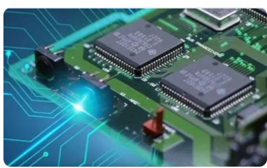
In addition to the simple concept of copying the circuit board, the copy PCB board also includes the decryption of some encrypted chips on the board, the reverse push of the PCB schematic diagram, the production of the BOM list, the PCB design and other technical concepts.
Reversal of PCB schematic
The schematic diagram is a drawing composed of electrical symbols used to analyze the principle of the circuit. It plays an indispensable role in the process of product debugging, maintenance, and improvement. The reverse design of the schematic diagram is the opposite of the forward design. The forward design is the design of the schematic first, and then the PCB design based on the schematic. The reverse design of the PCB refers to the reverse deduction of the product based on the existing PCB file or the actual PCB. Schematic diagram to facilitate the technical analysis of the product and to assist the later product prototype debugging production or improvement and upgrade.