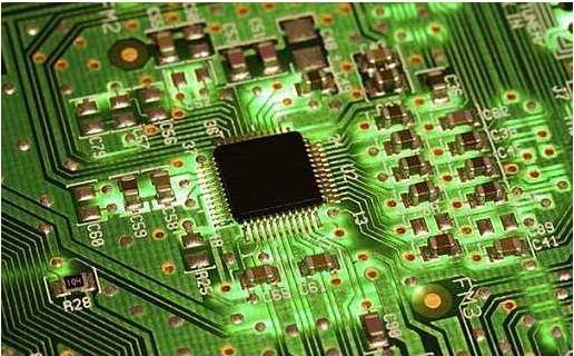
In the PCBA foundry processing process, the choice of PCBA tin penetration is very important. In the through-hole plug-in process, the PCB board has poor tin penetration, which can easily cause problems such as false soldering, tin cracks and even dropouts. We should understand these two points about PCBA through tin:
One, PCBA tin penetration requirements
According to the IPC standard, the PCBA tin penetration requirement of through-hole solder joints is generally more than 75%, that is to say, the tin penetration standard for the appearance inspection of the panel surface is not less than 75% of the hole height (board thickness), PCBA The tin penetration is suitable at 75%-100%. The plated through holes are connected to the heat dissipation layer or the heat conduction layer for heat dissipation, and the PCBA tin penetration requires more than 50%.
2. Factors affecting PCB tin penetration
The PCBA tin penetration is mainly affected by factors such as material, wave soldering process, flux, and manual soldering.
Specific analysis on the factors affecting PCBA tin penetration:

1. Material
Tin melted at high temperature has strong permeability, but not all metals to be welded (PCB boards, components) can penetrate in, such as aluminum metal, whose surface generally automatically forms a dense protective layer, and the internal molecules The difference in structure also makes it difficult for other molecules to penetrate. Second, if there is an oxide layer on the surface of the metal to be welded, it will also prevent the penetration of molecules. We generally use flux to treat it or brush it with gauze.
2. Flux
Flux is also an important factor affecting the poor tin penetration of PCBs. The flux mainly plays a role in removing the surface oxides of PCB and components and preventing re-oxidation during the soldering process. The selection of the flux is not good, the coating is uneven, and the amount is too small. Will lead to poor tin penetration. A well-known brand of flux can be selected, which will have higher activation and wetting effects, and can effectively remove difficult-to-remove oxides; check the flux nozzles, and the damaged nozzles need to be replaced in time to ensure that the PCB surface is coated with a proper amount of flux. Give full play to the flux effect of the flux.
3. Wave soldering
The poor solder penetration of PCBA is directly related to the wave soldering process. Re-optimize the soldering parameters with poor solder penetration, such as wave height, temperature, soldering time or moving speed. First, reduce the orbital angle appropriately and increase the height of the wave crest to increase the contact amount of liquid tin with the soldering end; then, increase the temperature of wave soldering. Generally speaking, the higher the temperature, the stronger the permeability of tin, but this should be considered. The components can withstand the temperature; finally, the speed of the conveyor belt can be reduced, and the preheating and soldering time can be increased, so that the flux can fully remove oxides, infiltrate the soldering ends, and increase the amount of tin consumed.
4. Manual welding
In the actual plug-in welding quality inspection, a considerable part of the weldment only has a taper on the surface of the solder, and there is no tin penetration in the via. The function test confirms that many of these parts are soldered. This situation is more common in manual plug-ins. During soldering, the reason is that the soldering iron temperature is not appropriate and the soldering time is too short. Poor solder penetration of PCBA can easily lead to false soldering problems and increase the cost of rework. If the requirements for PCBA tin penetration are relatively high and the welding quality requirements are stricter, selective wave soldering can be used, which can effectively reduce the problem of poor PCBA tin penetration.
When it comes to PCBA design, many people don't understand it. The PCBA design and processing is mainly aimed at small and medium enterprises and individuals who do not have their own design team. Transform the customer's ideas into practical concrete plans, optimize the implementation of the plan, finalize the draft and manufacture the products, and transform the customer's ideas into concrete physical products. This is the PCBA design and processing service.
The first is to have a professional design team fully communicate with customers, and understand the product's ideas, functions and appearance requirements clearly. The design team will give the corresponding PCBA design and processing according to the customer's needs, and optimize the plan after communicating with the customer and establish the final plan. After the plan is established, select the various components required by the product.
Then PCB design and processing will produce samples of the products in the plan, and professional engineers will analyze the samples and give PCB proofing files. Further optimize and upgrade products through documents, improve product quality, and reduce after-sales maintenance costs. After several product proofings, it is handed over to the customer for final confirmation. It is the PCB program design process.
Through the above introduction, I believe that everyone has a certain understanding of PCBA design and processing process. The design and processing of PCBA requires not only a professional design team, but also a lot of machinery and equipment to complete the assembly of an electronic board, and there are many links involved in manufacturing. High-quality manufacturers, the quality of machinery and equipment and manufacturing capabilities are very high. The products designed can often meet the needs of the market.