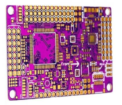
As civilian electronic products become more and more refined, the PCB as the carrier board of this type of product is getting more and more refined, and the lines are getting more and more dense.
In the PCB processing process, there are other regular defects due to different processes, for example, the filming phenomenon of the electrical board, the oxidation of the board surface, etc., all such regular defects need to be optimized according to the different AOI Disadvantages, with the application, give full play to the advantages of different types of AOI, so as to achieve better results, improve PCB detection capabilities, and effectively control product quality. As the frequency and speed of signal transmission become higher and higher, the circuit board quality The requirements of AOI are becoming higher and higher. At the same time, there will be impedance lines and non-impedance lines in a layer of graphics. The control of impedance lines is stricter than that of non-impedance lines. At the same time, we are in the process of AOI detection.

With the increase of the control stringency, the detection efficiency will be reduced correspondingly, and the detection cost will be increased. Automatic optical inspection equipment has been widely used in various industries.
In the PCB processing process, as an important testing equipment, key quality assurance tools are also widely used.The principle of AOI applied to PCB testingis: using various light sources to filter through optical lenses and irradiate them on the PCB to be tested. Then the reflected light (excitation light) passes through various filter lenses and is reflected on the receiver. The receiver generates a corresponding electrical signal according to the strength of the light signal. The PCB board graphic data stored by AOI itself is compared, and the defect is reported at the position of the difference. Finally, the inspector will confirm the processing to complete the entire inspection process. Take a picture of the surface graphics.
As we all know, the current digital technology has made rapid development. Compared with 10 years ago, it can be said that the pixels have increased by dozens of times or even hundreds of times.
Finding a digital camera with tens of millions of pixels on the market can be said to be simple; and the adaptability of PCB digital cameras is relatively strong, and the requirements for light contrast are relatively low, so that the adaptability of matrix imaging method AOI is enhanced. : On the other hand, the image taken by a digital camera is a planar image, which reduces the dependence on software; however, this method is still a newly developed technology, and further development and improvement are still needed. The quality lies in prevention and control. .
AOI is an important PCB inspection equipment. If it is only used to judge the quality of the product, it will not participate in quality prevention. In the control, it will lose the highest value of its inspection equipment. Decent, in order to improve product quality and prevent the graphics process from generating batches For non-conformity, reduce the cost of scrap and repair, you can use AOI to do the first quality inspection of the graphics process. In this process.
In order to prevent variations in the PCB graphics processing process, it is necessary to conduct inspections with zero-defect standards. As long as any graphics processing defects are found, they must be promptly fed back to the previous processing procedures. The previous procedures need to be confirmed and dealt with accordingly to avoid batch problems. In order to reduce the cost of repair and scrap.