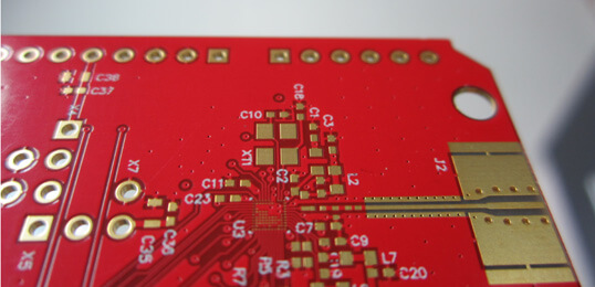
SMD,English name Surface Mounted Devices,it is a kind of SMT (Surface Mount Technology) electronic components. In addition, SMD components used for SMT do not have leads like through-hole components, and in terms of electrical function,SMD components used for SMT are no different from through-hole components, but SMDs are smaller in size and therefore have better electrical function.In the field of LED display, SMD package technology is a technology that encapsulates LED chips, brackets, leads and other components into miniaturised, pinless LED lamp beads and mounts these lamp beads directly onto printed circuit boards (PCBs) by means of an automated placement machine. Compared with the traditional DIP (double in-line package) technology, SMD package technology has a higher degree of integration, smaller size and lighter weight.
The most basic SMD surface mount device installation process mainly has the following steps:
Installation of the substrate: the substrate will be fixed on the countertop
Point paste or glue: according to the size of the electronic components,the SMD adhesive coated in a pre-determined position,if the assembly process using reflow soldering, it is necessary to apply the paste in the substrate pads,the current commonly used medium - high temperature level Sn-Ag solder paste.
Installation of SMD: Generally, an automated professional mounter is used, which mainly consists of:suction and loading head for picking and placing SMD, X-Y working table, program control system and feeding part.
Thermal curing: carried out after the dispensing and placement of SMD,the adhesive is cured by curing oven under certain temperature and time control.The curing process is carried out in a curing oven under a certain temperature and time control to improve the adhesive strength of the SMD,and to prevent the components from being shifted due to vibration and impact during storage and transportation.
SMD soldering:using SMD adhesive bonded wave soldering and solder paste bonded reflow soldering two ways.
Cleaning:Remove residual adhesive to prevent corrosion of the substrate.
Inspection and testing:Solderability is checked according to standards and test requirements.

SMD device reflow soldering device layout requirements
1) The same kind of SMD device spacing requirements ≥ 12mil (pad to pad), heterogeneous devices: ≥ (0.13 × h + 0.3) mm (h is the maximum height difference around the nearest neighboring devices).
2) The list of SMT device spacing for reflow process: (Distance value is measured by the larger of pads and device body).
3) When considering compatible replacements for SMD devices, overlap is allowed for new tiny components with no or short leads, overlap is allowed for patches and inserts, and overlap is not allowed for SOP devices.
4) A 3mm no-fabric zone is required around BGA devices, and a 5mm no-fabric zone is optimal. In the layout of the space density constraints, chip components are allowed to no-fabrication area of 2mm, but not preferred.Generally BGA is not allowed to be placed on the back; when the back of the BGA device, can not be placed on the front of the BGA 8mm no-fabrication zone within the projection.
5) Larger than 0805 package ceramic capacitors, the layout as close as possible to the transmission edge or less stressful areas, and its axial direction as far as possible parallel to the direction of transmission and the board.
6) The SMD should not be arranged within 3mm around the plug-in device or board edge connector to prevent damage to the device caused by the stress generated when the connector is plugged in or out.
7) The solder joints of the device should be easy to visually inspect, to prevent the higher devices arranged next to the lower devices to affect the detection of solder joints, the general requirements of the viewing angle of ≤ 45 degrees.
In the SMD package,the component pins are directly connected to the PCB (Printed Circuit Board) by soldering or gluing without inserting holes.One of the main advantages of this type of package is that it can greatly reduce the spacing between components,thus making the entire circuit board becomes more compact and space-saving.This is essential for today's increasingly compact electronic product designs.
In addition,SMD packaging can also improve the performance and reliability of the board. Since the pins of SMD components are directly connected to the PCB, the connection length between the pins is reduced, thus reducing the resistance and inductance of the circuit and improving the stability of signal transmission. In addition, the SMD packaging method can also reduce the number of welding points, reduce the impact of welding quality on the entire circuit, and improve the reliability of the circuit.
In practical applications,SMD package method has a wide range of components,including chip resistors, chip capacitors, chip inductors, SMD diodes, SMD transistors and so on. These components are widely used in a variety of electronic devices, such as cell phones,tablet PCs, televisions, medical devices, and so on. Since SMD packaging method has the advantages of small size, light weight,high efficiency, etc.,it is widely used in these electronic products.
Overall,SMD package method,as an advanced packaging technology, provides more possibilities for the design and manufacture of electronic products. It can not only improve the performance and reliability of the circuit board,but also make electronic products more compact and lightweight. With the development of electronic products in the direction of miniaturization, lightweight, high performance, SMD packaging will be more and more attention, and play an increasingly important role in the future of the electronics industry.