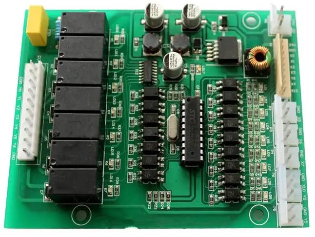
Reflow soldering is the final process of the production of fr4 pcb in the SMT section. Its defects include printing and mounting defects, including lack of tin, short circuit, side standing, offset, missing parts, multiple parts, wrong parts, reverse, reverse, monument, crack, tin bead, faulty soldering, hole, glossiness. Its neutral monument, crack, tin bead, faulty soldering, hole, glossiness are unique defects after welding.

Monument: the phenomenon that one end of the component leaves the pad and is inclined or upright upward.
Solder connection or short circuit: there is solder connection between two or more non-connected solder joints, or the solder of the solder joint is not connected with the adjacent wire.
Displacement/deviation: the element deviates from the predetermined position in the horizontal (horizontal), longitudinal (vertical) or rotation direction of the pad.
Empty welding: the solderable end of the component is not connected with the bonding pad.
Reverse direction: the direction of the polarity element is wrong when it is installed.
Wrong parts: the model and specification of the components attached at the specified position do not meet the requirements.
Less parts: materials are not pasted at the position where components are required.
Exposed copper: the green oil on the surface of PCBA falls off or is damaged, and the copper foil is exposed.
Blistering: PCBA/FR-4 PCB surface has regional expansion deformation.
Tin hole: after passing the furnace, there are blowholes and pinholes on the component solder joints.
Tin crack: tin surface crack.
Hole plugging: the solder paste remains in the plug hole/screw hole and other guide hole plugging.
Foot warping: The foot of the multi-pin component is warped and deformed.
Side standing: the side of the component welding end is directly welded.
False welding/false welding: the components are not welded firmly, and will have poor contact due to external or internal stress, which will be disconnected and connected.
Back/back: the component list is pasted on the other side of the fr4 pcb by screen printing, and the product name and specification screen printing font cannot be recognized.
Cold welding/non melting tin: the surface of the solder joint is not shiny, and the crystal is not completely melted to achieve reliable welding effect.
Steel mesh is also known as SMT Stencil, which is a special mold for SMT processing. Its main function is to help solder paste deposit; The purpose is to transfer the exact amount of solder paste to the corresponding position of the empty fr4 pcb. With the development of SMT technology, SMT steel mesh has also been widely used in rubber process such as red glue.
1. Chemical etching model
The template opening is formed by chemical etching, which is suitable for making brass and stainless steel templates, with the following characteristics:
1) The opening is bowl-shaped, and the release performance of solder paste is poor;
2) It can only be used for printing components with PITCH value greater than 20 mil, such as 25~50 mil;
3) The thickness of formwork is 0.1~0.5mm;
4) The size error of the opening is 1mil (position error);
5) The price is cheaper than laser cutting and electroforming.
2. Laser cutting template
Laser cutting is used for the last opening, which has the following characteristics:
1) The upper and lower openings are naturally trapezoidal, and the upper opening is usually 1~5mil larger than the lower opening, which is conducive to the release of solder paste;
2) The hole size error is 0.3~0.5mil, and the positioning accuracy is less than 0.12mil;
3) The price is more expensive than chemical etching and cheaper than electroforming;
4) The hole wall is not as smooth as the electroforming formwork;
5) The thickness of u5kemanzu formwork is 0.12-0.3mm;
6) Usually used for printing in fr4 pcb when the PITCH value of the component is 20mil or less.