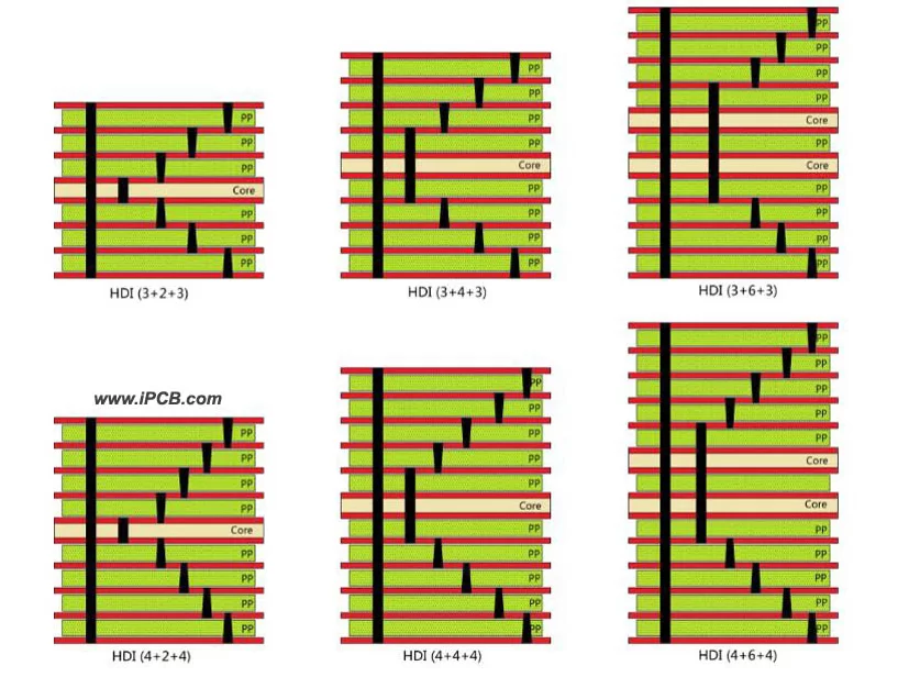
High Density Interconnect PCBs are mainly used in advanced interconnect applications because any two layers in the PCB can be interconnected without any restrictions. That is, any-layer technology offers greater layout flexibility and can save at least 30% of the PCB space. However, due to its technical complexity, the cost is higher than that of traditional laminated boards. There are many advantages and benefits of using HDI PCBs, such as high-speed performance, high frequency, and compact size. Their professionalism and characteristics are applied in many aspects, including personal computers, MP3 players, game consoles, and smartphones.
Types of High Density Interconnect PCBs:
1. Through-Hole HDI PCB
This type of HDI PCB is a combination of high-density interconnect and traditional through-holes. To achieve a higher wiring density, through-holes are sometimes combined with microvias. They are usually used in applications that require a balance between high-density wiring and through-hole component compatibility.
2. Sequentially Built HDI PCB
This is a type of HDI PCB manufactured by sequentially laminating multiple thin core materials. Each layer provides a unique circuit pattern and specification. This type of HDI PCB helps to form flexibility and layer thickness in the PCB according to specific requirements. They are also known as multilayer build-up HDI PCBs.
3. Rigid-Flex HDI PCB
In these PCBs, there are both rigid and flexible regions, mainly interconnected through microvias. The special feature of rigid-flex HDI helps to meet the needs where there is a great demand for three-dimensional wiring and lightweight design. They also take advantage of combining HDI technology with the flexibility of flexible PCBs or circuits.
4. Any-Layer HDI PCB
This is a PCB that extends to multiple layers with the help of microvias. This allows connections between layers in any combination. Due to the limited restrictions on layer interconnection, they also offer maximum wiring and interconnect flexibility. They are very suitable for high-performance applications that require strict signal integrity. They are also known as stacked microvia or stacked through-hole HDI PCBs.
5. Build-Up HDI PCB
They are characterized by a coreless structure and are constructed using thin dielectric layers and copper. Then, with the help of microvias, they form circuits. They are known as coreless HDI PCBs.
6. Cavity-Based HDI PCB
In this type of HDI PCB, they include cavities in the board itself in the structure to accommodate components and connections. The purpose of such cavities is to help achieve miniaturization and integration of components, thus introducing a more streamlined design for the PCB. They are very suitable for areas where space management is crucial.

High-Density Interconnect
Characteristics of High Density Interconnect PCBs:
1. More Layers
The number of layers of high-density interconnect PCBs always exceeds two. They are usually between four and ten layers, and sometimes even more than ten layers. These layers give us the advantage of generating more wiring options and also help to place through-holes within the circuit board. This will result in an increased overall wiring density of the circuit board.
2. Microvias
Microvias allow the coupling of traces between multiple layers of the PCB without the need for a large drill size, enabling denser wiring and finer components. High-density interconnect PCBs utilize these microvias, which are tiny plated-through holes with a width of less than 150 microns.
3. Buried Vias and Blind Vias
High-density interconnect PCBs can include blind vias in addition to traditional through-holes. In blind vias, the connection is usually made on the outer layer and connected to one or more inner layers. On the other hand, there is also buried vias that connect inner layers and do not penetrate the board thickness. In both types of vias, they help to reduce signal interference and also help to achieve additional complex configurations in wiring.
4. Enhanced Signal Integrity
In high-density interconnect PCBs, there is always only a small amount of electromagnetic interference and signal distortion. This is mainly because of the use of vias such as microvias, blind vias, and buried vias. The use of these vias in HDI will enhance signal integrity in radio frequency and digital applications that require high speed.
Applications of High Density Interconnect PCBs:
1. Portable Devices
Due to the ability of HDI PCBs to densely install components within a small area and their compact size, they are widely used in applications such as smartphones, wearable electronics, and tablets. Despite their small size and design, HDI PCBs still possess high performance and functionality.
2. Data Storage and Computing
Using HDI PCBs in high-performance data storage devices and computing systems will benefit from achieving high processing speed, as well as improving signal strength and integrity. HDI helps to integrate complex circuits and dense memory modules.
3. Automotive Industry
Modern vehicles use a large number of electronic systems during the assembly process. Nowadays, HDI PCBs have been integrated into numerous applications in automobiles, including infotainment, GPS, autonomous driving assistance, and the overall safety of the vehicle. Typical applications in automobiles, such as collision avoidance systems, cruise control, ABS, and infotainment systems, extensively use HDI PCBs.
4. Industrial Applications
In the automation industry and robot systems, we need to use compact and complex electronic technologies to achieve high-end industrial production and manufacturing. The use of HDI PCBs helps to integrate sensors, actuators, and communication interfaces in industrial equipment.
5. Telecommunications
Communication protocols, including base stations, routers, transmitter network devices, etc., rely on HDI PCBs to achieve better performance and enhanced communication. It helps to achieve high-rate data transmission, improve signal processing, and overall wireless communication. This can reduce the occupied space.
In conclusion, High Density Interconnect PCBs contribute to electronic manufacturing with many advantages such as miniaturization and optimization of circuit board performance, improvement of electrical performance, efficient space utilization, enhancement of reliability, and increase of design flexibility.