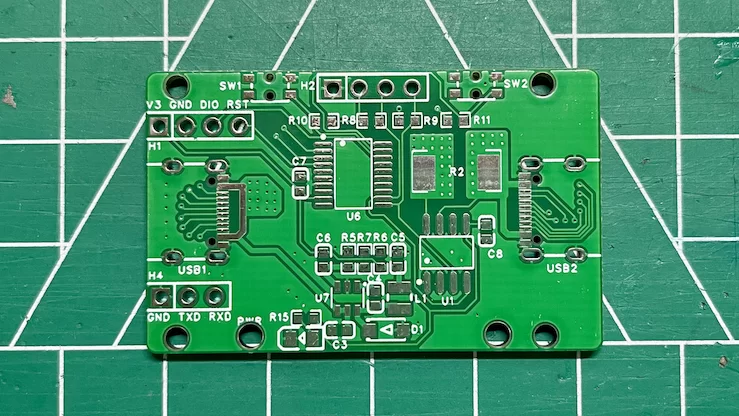
How to DIY PCB Board?This article will show you how to make a PCB board.In production, electronic parts are often used to connect sensors and control various devices. A breadboard can only be used as a temporary experimental circuit board, and universal board wiring is messier. The best solution is to make your own PCB. The following is a practical experience sharing in the production of a PCB. Although it cannot compare with factory production technology, it is sufficient for amateur production. Due to technical and equipment limitations, only the simplest single-panel can be produced.
DIY PCB Board mainly involves four steps: circuit board design, curing, etching, and drilling.
First,design a good circuit, set up parts, connectors, etc. If necessary, a breadboard can be used to test the circuit. Once the circuit is determined to be correct and feasible, you can start making the PCB. It is recommended to use Circuit Maker (a free PCB design software) that allows you to draw schematics, featuring a library of commonly used parts, making it very convenient. Once the schematic is drawn, the software will convert the schematic parts and wiring into a PCB layout. If you don't need to draw a schematic, you can directly proceed with PCB design, adding your own wiring and solder pads. Ensure to draw the design as a top view and arrange placements accordingly, such as adding text and setting it to mirror for reverse.

DIY PCB Board
DIY PCB Board involves printing the circuit lines onto a photopolymer-coated circuit board using a curing lamp. Design the PCB with a top view, and when printing the circuit diagram, set it to mirror for reverse left and right. The PCB negative should be printed in the darkest color and maintain a 1:1 ratio on a transparent film. A laser printer or photocopier that directly prints PDF files is most suitable. The toner must be sufficient, and high-temperature printing film should be used. It is best to manually feed the film into the printer.Prepare a pre-cut size of the PCB copper plate. I have tried applying the photopolymer myself, but the result was not good and uneven, so I ended up purchasing Kinsten gold electronic photopolymer PCB, which is guaranteed in quality and convenient. A light box with a curing lamp is needed for the curing process. The power, distance, and exposure time of the lamp should be carefully set. I use three T5-6W curing lamps; three lamps will produce better results, complementing each other and making the lines more distinct. Be sure to use a piece of transparent adhesive plate to compact the PCB negative and the PCB, ensuring no gaps. The film should be placed 5 cm from the curing lamp and exposed for 9 minutes (this time was determined through testing and can be adjusted).
DIY PCB Board etching involves removing unwanted copper foil, leaving behind the needed circuit lines. This process requires three chemicals: developer powder, etching powder, and stripping powder. Developer powder and etching powder can be found at the largest electronic parts store in Apliu Street, Sham Shui Po.Dissolve 5 grams of developer powder in 100 ml of water in a dish and place the exposed PCB in it. Gently shake for a few minutes until the lines are clearly visible. Once the lines appear completely, immediately remove the PCB and rinse with water. If there is any damage to the lines, dry the base plate and repair it with an oil-based pen.Next, clean the dish and dissolve 45 grams of environmental protection etching powder in 150 ml of hot water (ensure the portion is not too small, or the etching concentration will not be sufficient later). Occasionally shake gently for about 40-60 minutes until complete. Remove the PCB and rinse with water.Finally, clean the dish and dissolve a small amount of stripping powder in a small amount of water. Place the PCB in it, and the protective film will instantly dissolve, revealing the copper foil lines. If stripping powder is not available, you can try a light oxidation solution.
Drill holes in the solder pads. Common hole diameters are 0.8 mm and 1 mm. The necessary tool is a small, lightweight electric drill.If you want to produce a large number of PCBs, you can first DIY a single PCB. Once successful, you can send the design file to a factory for production. This process requires careful study of PCB design software and industry-accepted file specifications.
DIY PCB Board production may not compare to factory technology, but it is sufficient for amateur enthusiasts.