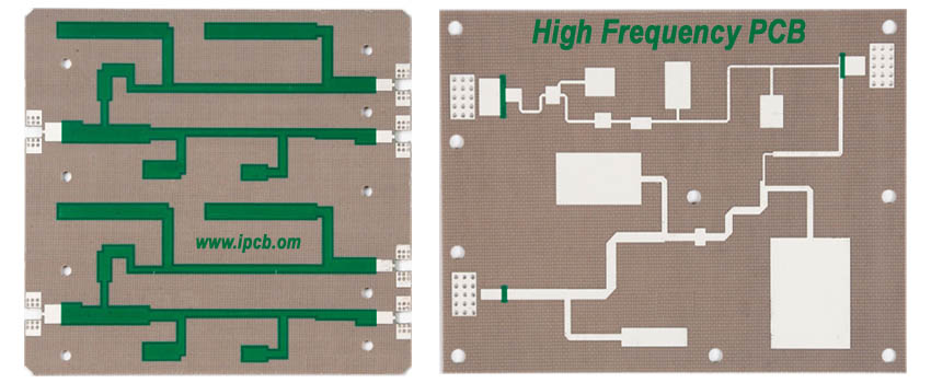
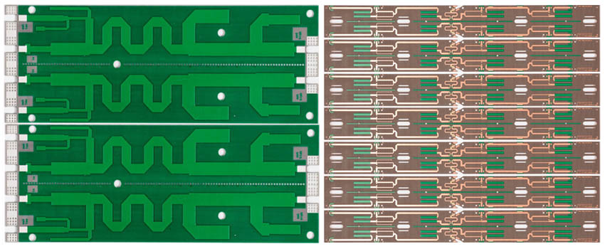
Product: high frequency PCB
Material: high frequency PCB materials
Quality standard: IPC 6012 Class2
high frequency pcb dk: 2.0 -1.6
Layers: 1 Layer pcb - 36 layer pcb
Thickness: 0.254mm - 12mm
Copper thickness: base copper 0.5oz / 1oz
Surface technology: Silver, Gold, OSP
Special process: mixed material, stepped groove
Application: High Frequency PCB, microstrip antenna
What is High Frequency PCB?
High frequency PCB manufacturer considers frequency board PCB made with high frequency PCB materials to be high frequency PCB. For example, Arlon PCB, Rogers PCB, Taconic PCB, isola PCB, Nelco PCB... It is a PCB produced by using some processes of PCB manufacturing method on high frequency PCB material or special high frequency PCB manufacturing method.
High frequency PCB design engineers believe that the PCB of high frequency circuit cooperation is high frequency PCB, High frequency PCB design engineers believe that the PCB of high frequency circuit cooperation is high frequency PCB. High frequency circuit refers to that when the frequency band is greater than 1GHz, it can be called high frequency circuit. High frequency circuit is basically composed of passive components, active devices and passive networks. Passive components or passive networks in high-frequency circuits mainly include high-frequency oscillation circuits, high-frequency transformers, resonators and filters, which complete the functions of signal transmission, frequency selection and impedance transformation.
With the rapid development of science and technology, more and more equipment are designed for applications above microwave frequency band (>1GHz) and even millimeter wave field (30GHz), which also means that the frequency is higher and higher, and the requirements for high frequency PCB substrate are higher and higher. For example, the substrate material needs to have excellent electrical properties and good chemical stability. With the increase of power signal frequency, the loss on the substrate is very small. With the emergence of 5g signal, the importance of high frequency PCB material is highlighted.

High Frequency PCB
Characteristics of high frequency PCB
1. High frequency PCB DK DF should be small and stable enough. Generally, the smaller the better. High Dk may cause signal transmission delay. This mainly affects the quality of signal transmission, and a smaller DF can reduce the signal loss accordingly.
2. The coefficient of thermal expansion of high frequency PCB should be the same as that of copper foil as far as possible, because the difference will lead to the separation of copper foil during cold and heat changes.
3. In humid environment, the water absorption of high frequency PCB must be low and high, which will affect PCB DK and DF.
4. High frequency PCB must have good heat resistance, chemical resistance, impact resistance and peel resistance.
Points for attention in high frequency circuit board manufacturing
1. At present, the most commonly used high-frequency is fluorine dielectric substrate, such as PTFE PCB, which is usually called Teflon PCB
2. Due to the special plate, the adhesion of PTH copper precipitation of high frequency PCB materials is not high. Usually, the via and surface need to be roughened with the help of plasma treatment equipment to increase the adhesion between PTH hole copper and solder resist ink.
3. High frequency board PCB cannot be ground before resistance welding, otherwise the adhesion will be very poor and can only be roughened with micro etching solution.
4. Most of the high frequency PCB materials are Teflon PCB materials. Forming with an ordinary milling cutter will have many burrs, and a special milling cutter is required.
5. High frequency PCB board has very high requirements for physical performance, accuracy and technical parameters. It is commonly used in automobile anti-collision system, satellite system, radio system and other fields.
6. High frequency PCB has strict requirements for PCB impedance control, which is very strict relative to line width control, with a general tolerance of about 2%.
High frequency PCB layout
1. High frequency circuits tend to have high integration and high layout density. The use of multi-layer high-frequency PCB is not only necessary for layout, but also an effective means to reduce interference.
2. The less lead bending between pins of high-speed circuit devices, the better. The lead of high-frequency PC blayout is preferably a full straight line, which needs turning. It can be turned by 45 ° broken line or circular arc. Meeting this requirement can reduce the external transmission and mutual coupling of high-frequency signals.
3. The shorter the lead between the pins of high-frequency circuit devices, the better.
4. The less lead layer alternation between pins of high frequency circuit devices, the better. The so-called "the less interlayer alternation of leads, the better" refers to the fewer vias (via) used in the process of component connection. It is measured that one via can bring about 0.5 pf distributed capacitance, and reducing the number of vias can significantly improve the speed
5. In the layout of high-frequency circuit, attention shall be paid to the "cross interference" introduced by the close parallel routing of signal lines. If parallel distribution cannot be avoided, a large area of "ground" can be arranged on the reverse side of parallel signal lines to greatly reduce the interference. Parallel routing in the same layer can hardly be avoided, but in two adjacent layers, the routing direction must be perpendicular to each other.
6. Implement the ground wire surrounding measure for the particularly important signal line or local unit, that is, draw the outer contour of the selected object. With this function, the so-called "land wrapping" processing can be automatically carried out for the selected important signal line. Of course, it will be very beneficial to the high-speed system to use this function for local land wrapping processing of clock and other units.
7. All kinds of signal routing in the high-frequency circuit board cannot form a loop, and the ground wire cannot form a current loop.
8. A high frequency decoupling capacitor shall be set near each integrated circuit block.
9. When connecting analog ground wire and digital ground wire to public ground wire, high-frequency choke link shall be used. When actually assembling high-frequency choke link, high-frequency ferrite beads with wires through the center hole are often used, which are generally not expressed in the circuit schematic diagram of high-frequency PCB, resulting in a network table (netlist. Does not contain such components, so its existence will be ignored during layout. In view of this reality, it can be regarded as an inductance in the schematic diagram, and a component package can be defined separately for it in the PCB component library. Before layout, it can be manually moved to a suitable position close to the confluence point of common ground wires.
10. Analog circuit and digital circuit shall be arranged separately. After independent layout, the power supply and ground shall be connected at a single point to avoid mutual interference.
11. Before DSP, off chip program memory and data memory are connected to the power supply, filter capacitors shall be added and kept as close as possible to the chip power pin to filter out power noise. In addition, shielding is recommended around key parts such as DSP, off chip program memory and data memory to reduce external interference.
12. The off chip program memory and data memory shall be placed as close as possible to the DSP chip. At the same time, they shall be reasonably arranged to make the length of data line and address line basically consistent. Especially when there are multiple memories in the system, it shall be considered that the clock input distance from the clock line to each memory is equal or a separate programmable clock drive chip can be added. When making the PCB printed circuit board of DSP hardware system Pay special attention to the correct and reasonable layout of important signal lines such as address line and data line. During layout, try to make the high-frequency line short and thick, and keep away from easily disturbed signal lines, such as analog signal lines. When the circuits around DSP are complex, it is recommended to make DSP and its clock circuit, reset circuit, off chip program memory and data memory into a minimum system to reduce interference Interference.
13. After mastering the skills of using the high frequency PCB layout design tool, after manual layout, in order to improve the reliability and producibility of high frequency circuit PCB, it is generally necessary to use advanced PCB simulation software for simulation.

High frequency PCB
iPCB products of high-frequency PCB mainly include Rogers PCB, Microwave PCB, radar PCB, RF PCB, microstrip PCB, antenna PCB, heat dissipation PCB, arlon PCB, mixed laminated PCB, f4b PCB, ceramic PCB and induction PCB
Which are applied to slot antenna, RF antenna, broadband antenna, frequency scanning antenna, microstrip antenna, ceramic antenna Power divider, coupler, combiner, power amplifier, dry amplifier, base station, etc.
The high frequency materials in stock of iPCB include, Rogers, Arlon, Taconic, isola, Panasonic, TUC, ITEQ, Shengyi, Wangling, Nelco, Doosan, Nanya, Ventec, EMC, Hitachi.
iPCB has professional high frequency PCB manufacturing experience, and provides high frequency PCB design rules, high frequency PCB layout to customers.
Product: high frequency PCB
Material: high frequency PCB materials
Quality standard: IPC 6012 Class2
high frequency pcb dk: 2.0 -1.6
Layers: 1 Layer pcb - 36 layer pcb
Thickness: 0.254mm - 12mm
Copper thickness: base copper 0.5oz / 1oz
Surface technology: Silver, Gold, OSP
Special process: mixed material, stepped groove
Application: High Frequency PCB, microstrip antenna
For PCB technical problems, iPCB knowledgeable support team is here to help you with every step. You can also request PCB quotation here. Please contact E-mail sales@ipcb.com
We will respond very quickly.