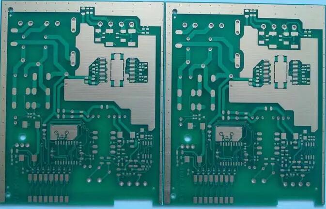
The hardware and software that power today’s electronic devices have developed at an extremely fast rate, but there is still a critical bottleneck-prototype design, especially the unforeseen and costly delays in the development process of PCB and PCBA circuit boards, as a response, 3D printing is now used to produce professional PCB boards and PCBA circuit boards, providing advantages in saving time, cost and innovation.
Although 3D printing PCB is being used in various professional and hobbyist applications, it is only recently that we have seen the development of this technology in electronic products such as PCB boards.
In each stage of product development, electronic designers and engineers must take out prototype boards for testing. The current standard subtractive manufacturing of PCBs is a multi-stage process, which is labor and material intensive and often outsourced.

During the design and testing process, the time spent waiting for a complex prototype may increase by several weeks instead of rapid prototyping. In addition, if the prototype shows any defects, the redesign will require additional days or weeks before the design is put into production Previous tests were tested, thereby bringing commercial risks to on-time product development. Printers can also save money and even allow users to create models that are usually difficult or impossible to produce. PCBA or models that are time-consuming using the current manufacturing process. In the end, The quality of the final product can be improved, and a whole new electronic world can even be produced.
The substrate of the PCB board itself is made of insulating and heat-insulating materials that are not easy to bend. The small circuit material that can be seen on the surface is copper foil. The copper foil is originally covered on the entire PCB board, but in the manufacturing process Part of it is etched away, and the remaining part becomes a network of fine lines. These lines are called wires or wiring and are used to provide circuit connections for parts on the PCB.
Usually, the color of the PCB board, PCB circuit board is green or brown. This is the color of the solder mask, which is an insulating protective layer, which can protect copper wires and prevent parts from being soldered to incorrect places. Now the motherboard and graphics card Multi-layer boards are used on the board, which greatly increases the area that can be wired.
1, multi-layer boards use more single or double-sided wiring boards, and put a layer of the insulating layer between each layer of boards and press them together.
2. The number of PCB layers means that there are several independent wiring layers. Usually, the number of layers is an even number and includes the outer two layers. Common PCB boards generally have a structure of 4 to 8 layers. Many PCB chip factories The number of layers can be seen by looking at the cut surface of the PCB board, but in fact, no one can have such good eyesight.
3. The circuit connection of PCB multilayer board and PCBA multilayer board is through the buried hole and blind hole technology. The mainboard PCB and display card mostly use a 4-layer PCB board, and some use 6 layer PCB, 8 layer PCB, or even a 10-layer PCB board.
4. If you want to see how many layers the PCB has, you can identify it by observing the guide holes, because the 4-layer board used on the motherboard and the display card is the first and fourth layers of wiring, and the other layers have other uses ( Ground wire and power supply), so, like the double-layer board, the via hole will penetrate the PCB board.