

The initial emergence of Wafer level packaging was driven by the manufacturing of low-speed I/O and low-speed transistor components for mobile phones, such as passive on-chip sensors and power transmission ICs. Currently, WLP is in a developmental stage, propelled by applications like Bluetooth, GPS, and sound cards, leading to a gradual increase in demand. As the industry progresses to the production stage of 3G mobile phones, various new applications for mobile phones are expected to become another growth driver for WLP, including TV tuners, FM transmitters, and stack memories. With memory device manufacturers gradually implementing WLP, it will lead to a standardized transformation of the entire industry.
Currently, this technology is widely used in various fields such as flash memory, EEPROM, high-speed DRAM, SRAM, LCD drivers, RF devices, logic devices, power/battery management devices, and analog devices (regulators, temperature sensors, controllers, operational amplifiers, power amplifiers). Wafer level packaging mainly adopts two basic technologies: thin-film redistribution and bump formation. The former is used to convert the bonding areas distributed along the periphery of the chip into bump bonding areas distributed in a planar array form on the chip's surface. The latter is used to create bumps on the bump bonding area, forming a bump array.

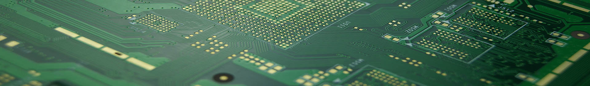
Wafer level packaging
Currently, there are three paths for Wafer level packaging: WLCSP, FOWLP, and PLP:
WLCSP (Wafer Level Chip Size Package), also known as fan-in WLP, is the traditional packaging method for final chip dicing. It is suitable for integrated circuits with a small number of pins. As the number of IC output signals increases, the solder ball size becomes more stringent. The PCB cannot meet the requirement of adjusting the size of the packaged IC and the position of the signal output pins.
FOWLP starts with chip dicing and then redistributes them onto new man-made molded wafers. Benefits include reduced package thickness, increased fan-out (more I/O interfaces), better electrical performance and better heat resistance. FIWLP and FOWLP have different applications, but both are the dominant packaging methods of the future. FIWLP is most widely used in analog and mixed-signal chips, followed by wireless interconnects, and CMOS image sensors are also packaged using FIWLP technology. FOWLP will be used primarily for processor chips in mobile devices.
PLP (Panel Level Packaging) is similar to FOWLP in that it redistributes chips onto larger rectangular panels rather than round wafers. The larger area means more cost savings and higher packaging efficiency. In addition, cutting chips into squares leads to wasteful wafer packaging, which rectangular panels can effectively address. However, this also puts higher demands on lithography and alignment. The basic idea is to complete chip fabrication at the same time as direct packaging on silicon wafers, packaging multiple chip units in an overall package structure. This avoids the step of individually packaging each chip in conventional packaging, thereby increasing productivity and reducing costs.
The process of Wafer level packaging typically includes the following steps:
Wafer Preparation: Cleaning and preparing the silicon wafer to ensure the reliability and consistency of the packaging process.
Package Structure Formation: Applying a layer of packaging material, usually a polymer, on the silicon wafer to form the basis of the package structure.
Circuit Connection: Creating metal wires (wire bonding) or other circuit connection structures on the silicon wafer to connect the chip's circuits to the package structure.
Testing and Quality Verification: Conducting electrical performance tests, package integrity tests, etc., to ensure that the packaged chips meet quality requirements.
Chip Separation: Separating the packaged chips from the silicon wafer to obtain individual packaged chips.
WLP is based on BGA technology and is an improved and enhanced form of CSP, fully reflecting the technical advantages of BGA and CSP. It has many unique advantages:
High packaging processing efficiency: It is manufactured using batch production processes in wafer form.
It inherits the advantages of flip-chip packaging, i.e., lightweight, thin, short, and small.
Low production facility costs: It can fully utilize the chip manufacturing equipment, avoiding the need to invest in separate packaging production lines.
Unified chip and packaging design consideration: Design efficiency is improved, and design costs are reduced.
Reduced production cycle: It significantly shortens the entire process from chip manufacturing, packaging to product delivery, leading to cost reduction.
Cost-effectiveness: The cost of WLP is closely related to the number of chips on each wafer. The more chips on the wafer, the lower the cost of that. This packaging is the smallest and lowest-cost packaging method.
The advantage of WLP lies in its applicability to chip-level packaging (CSP) technology for smaller integrated circuits. By adopting parallel packaging and electronic testing technology at the wafer level, WLP significantly reduces chip area while increasing production yield. Additionally, the cost per I/O is greatly reduced by conducting chip connections in parallel at the wafer level. Furthermore, simplified die-level testing procedures further reduce costs.
Utilizing Wafer level packaging enables chip packaging and testing to be achieved at the wafer level.


