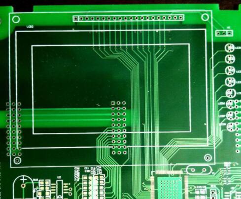
Nowadays, electronic products are thin and short. With the development trend of pursuing higher signal transmission quality, the size of circuit board is becoming smaller and smaller, and the routing density of each layer is becoming larger and larger. Especially when the signal speed continues to accelerate, the problem of crosstalk is becoming more and more serious. Crosstalk will directly affect whether the signal can be received correctly. Therefore, how to reduce noise interference has become an important topic for PCB design team.
This paper will explain in detail how to use the IDA (in design analysis) crosstalk analysis function in Allegro? PCBdesigner through design examples. As long as it is matched with the mounting of part models, EE / layout personnel can conduct Si level crosstalk analysis synchronously in the design, eliminate common signal crosstalk problems in advance, achieve more results, and improve the design efficiency, The adverse probability is reduced.

1. Crosstalk challenge
When we are in a low partition office environment, if there are just a few excited and engaged colleagues around us, we are easy to receive sound pressure sources from different directions. Sometimes, when several people in the same direction sound at the same time, the influence of sound pressure will be more multiplied and felt. When this situation occurs in electronic product design, it is a common crosstalk problem!
Crosstalk, also known as crosstalk interference, in short, is the inductive / capacitive coupling phenomenon between two transmission lines. When the signal is on the active line or aggressive line, it will transfer part of the signal to the static line without signal (also known as victimline), resulting in the problem of coupling interference. In the example shown in figure (1) below, the working voltage of the attack line next to the injured line is either 1V or 2.5V. Due to different intensities, their influence on the coupling noise of the injured or static line will also be different.
Nowadays, electronic products are thin and short. With the development trend of pursuing higher signal transmission quality, the size of circuit board is becoming smaller and smaller, and the routing density of each layer is becoming larger and larger. Especially when the signal transmission speed continues to accelerate, the crosstalk problem is becoming more and more serious. How to reduce noise interference has become an important issue for PCB design team.
2. Ways to suppress crosstalk
Crosstalk directly affects whether the signal can be received correctly, which is a thorny problem for PCB design! In order to reduce crosstalk, some will use the 3W rule specification to ensure that the line spacing is enough to avoid mutual interference. However, as we mentioned in skill 2 - coupling, the 3W rule is audited only by spacing, which has the disadvantage of insufficient accuracy and easy to increase the cost.
When we take a closer look at crosstalk analysis, different operating voltage levels will have different influence intensities. Under different phase combinations, some may be reversed and have the opportunity to reduce or even offset, some may be more amplified due to the influence of in-phase, or the high or low level with the affected line will also have different anti-interference degrees. Therefore, we need to analyze and check various interference settings, but the accuracy of different methods will vary. As shown in figure (2) below, the higher the accuracy of the way to the right, that is, estimated xtalk and simulated xtalk. However, the behavior of parts can be achieved only when models are attached to parts to achieve more accurate results.
Therefore, for PCB design, in addition to the coupling signal quick screen inspection previously introduced, if a more detailed signal crosstalk analysis is required due to different intensities / behaviors of interference sources, if there can be an auxiliary analysis tool, as long as the part model is mounted, the analysis will have the characteristics of the part model, and the above situations will be considered, We can conduct Si level crosstalk analysis synchronously in the design and achieve more results without relying on Si personnel, so as to improve the design efficiency and reduce the adverse probability.